Semiconductor device

a semiconductor device and metal insulator technology, applied in the direction of semiconductor devices, electrical devices, transistors, etc., can solve the problems of low work function unable to have a eff of about 3.9 to 4.3 ev suitable for n-channel mis transistors, and generally low resistance to etching solution of the layer containing the group iia and iiia metallic elements

Inactive Publication Date: 2009-12-31
TOSHIBA MEMORY CORP
View PDF5 Cites 9 Cited by
  • Summary
  • Abstract
  • Description
  • Claims
  • Application Information

AI Technical Summary

Problems solved by technology

However, a metal having a low work function suitable for the n-channel MIS transistor is generally not stable in a heat treatment step necessary for a transistor formation process, and cannot have a φeff of about 3.9 to 4.3 eV suitable for the n-channel MIS transistor especially on the high-k gate insulating film after the formation of the transistor.
However, the layer containing the groups IIA and IIIA metallic elements is generally low in resistance to an etching solution (e.g., refer to H. Y. Yu et al., Tech.

Method used


Image

  • Semiconductor device
  • Semiconductor device
  • Semiconductor device

Examples


first embodiment

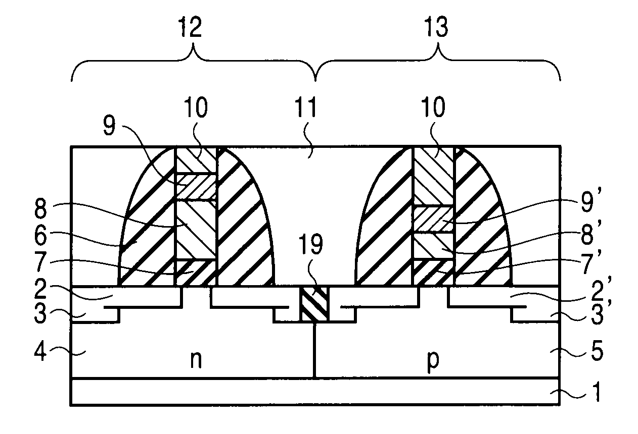
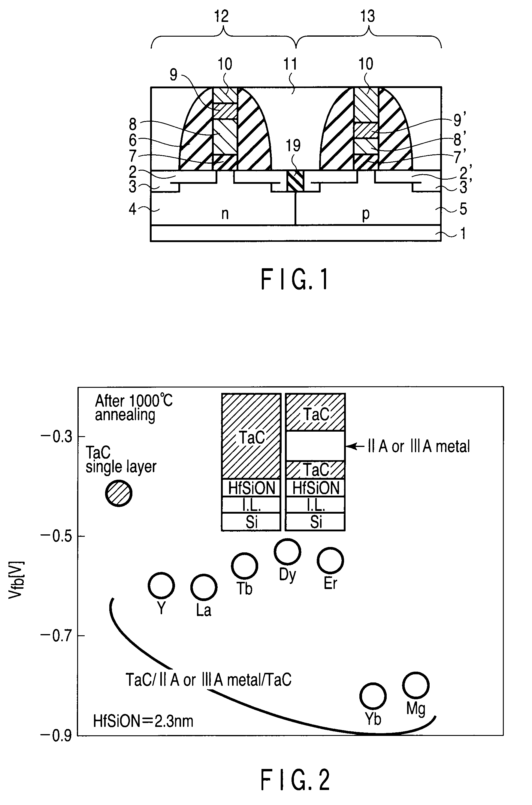
[0046]FIG. 1 is a sectional view of a semiconductor device according to a first embodiment of the present invention. An n-type semiconductor region 4 and a p-type semiconductor region 5 which are insulated from each other by a shallow trench isolation (STI) 19 are provided in a surface region of an Si substrate 1 as a semiconductor substrate. A p-channel MISFET 12 and an n-channel MISFET 13 are formed in the respective semiconductor regions. The n- and p-type semiconductor regions 4, 5 are formed as so-called wells.

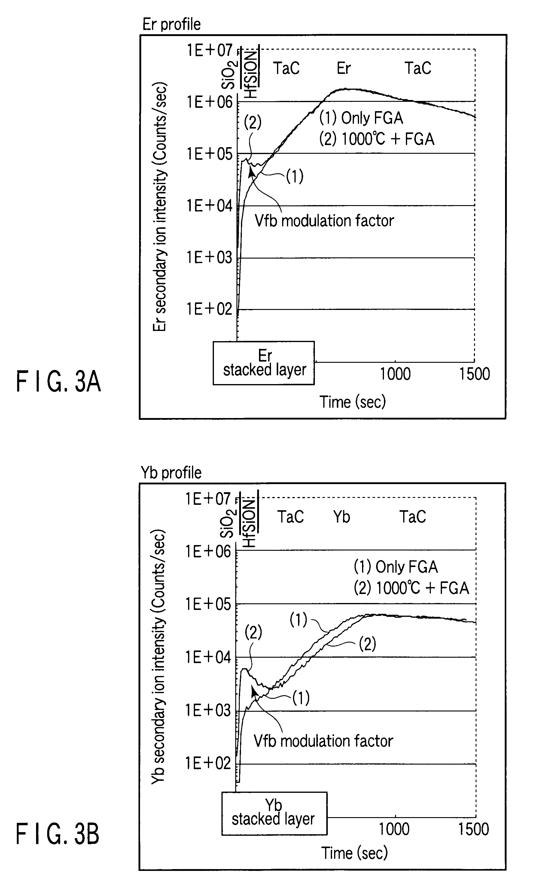
[0047]A high-k gate insulating film (dielectric) 7 such as HfSiON is formed on the surface of the n-type semiconductor region 4. A gate insulating film 7′ is formed on the surface of the p-type semiconductor region 5, and this gate insulating film 7′ is based on a high-k gate insulating film such as HfSiON and contains at least one of groups IIA and IIIA metallic elements (e.g., Mg, Ca, Sr, Ba, Sc, Y, La, Ce, Pr, Nd, Pm, Sm, Eu, Gd, Tb, Dy, Ho, Er, Tm, Yb, Lu).

[0048]In ad...

second embodiment

[0077]FIG. 14 is a sectional view of a semiconductor device according to a second embodiment of the present invention. An n-type semiconductor region 4 and a p-type semiconductor region 5 are provided in a surface region of an Si substrate 1 as a semiconductor substrate. A p-channel MISFET 12 and an n-channel MISFET 13 are formed in the respective semiconductor regions. The n- and p-type semiconductor regions 4, 5 are formed as so-called wells.

[0078]A high-k gate insulating film 7 such as HfSiON is formed on the surface of the n-type semiconductor region 4. A gate insulating film 7′ is formed on the surface of the p-type semiconductor region 5, and this gate insulating film 7′ is based on a high-k gate insulating film such as HfSiON and contains at least one of groups IIA and IIIA metallic elements.

[0079]A lower gate electrode layer 14 based on, for example, TaCx is formed on the gate insulating film 7 located on the n-type semiconductor region. A lower gate electrode layer 8 based ...


PUM


Abstract

A semiconductor device includes pMISFET and nMIS formed on the semiconductor substrate. The pMISFET includes, on the semiconductor substrate, first source / drain regions, a first gate dielectric formed therebetween, first lower and upper metal layers stacked on the first gate dielectric, a first upper metal layer containing at least one metallic element belonging to groups IIA and IIIA. The nMISFET includes, on the semiconductor substrate, second source / drain regions, second gate dielectric formed therebetween, a second lower and upper metal layers stacked on the second gate dielectric and the second upper metal layer substantially having the same composition as the first upper metal layer. The first lower metal layer is thicker than the second lower metal layer, and the atomic density of the metallic element contained in the first gate dielectric is lower than the atomic density of the metallic element contained in the second gate dielectric.

Description

CROSS-REFERENCE TO RELATED APPLICATIONS[0001]This application is based upon and claims the benefit of priority from prior Japanese Patent Application No. 2008-169074, filed Jun. 27, 2008, the entire contents of which are incorporated herein by reference.BACKGROUND OF THE INVENTION[0002]1. Field of the Invention[0003]The present invention relates to a structure of a complementary metal insulator semiconductor device (CMIS) using a metal gate electrode, and a manufacturing method thereof.[0004]2. Description of the Related Art[0005]In order to meet the requirements for an effective reduction in the thickness of a gate insulating film associated with increasing performance and increasing integration of semiconductor devices, it will be necessary in the future to introduce the technique for a metal gate electrode and a high dielectric (high-k) gate insulating film. To obtain proper performance in a CMIS transistor (cMISFET) using the metal / high-k gate insulating film, an effective work ...

Claims


Application Information

Patent Timeline
Patent Type & Authority Applications(United States)
IPC IPC(8): H01L27/092H01L21/8238
CPCH01L21/823842H01L27/092H01L29/6659H01L29/518H01L29/4966
Inventor ICHIHARA, REIKAKOYAMA, MASATO
Owner TOSHIBA MEMORY CORP
Why Eureka
Try Eureka