
Compliant Substrate In Particular For Hetero-Epitaxial Depositing

a substrate and hetero-epitaxial technology, applied in the field of substrates, can solve the problems of hetero-epitaxial stress release, limit the number and diversity of layers, and poor quality of the growth of layers,

Inactive Publication Date: 2009-12-17
COMMISSARIAT A LENERGIE ATOMIQUE ET AUX ENERGIES ALTERNATIVES
View PDF14 Cites 8 Cited by
  • Summary
  • Abstract
  • Description
  • Claims
  • Application Information

AI Technical Summary

Benefits of technology

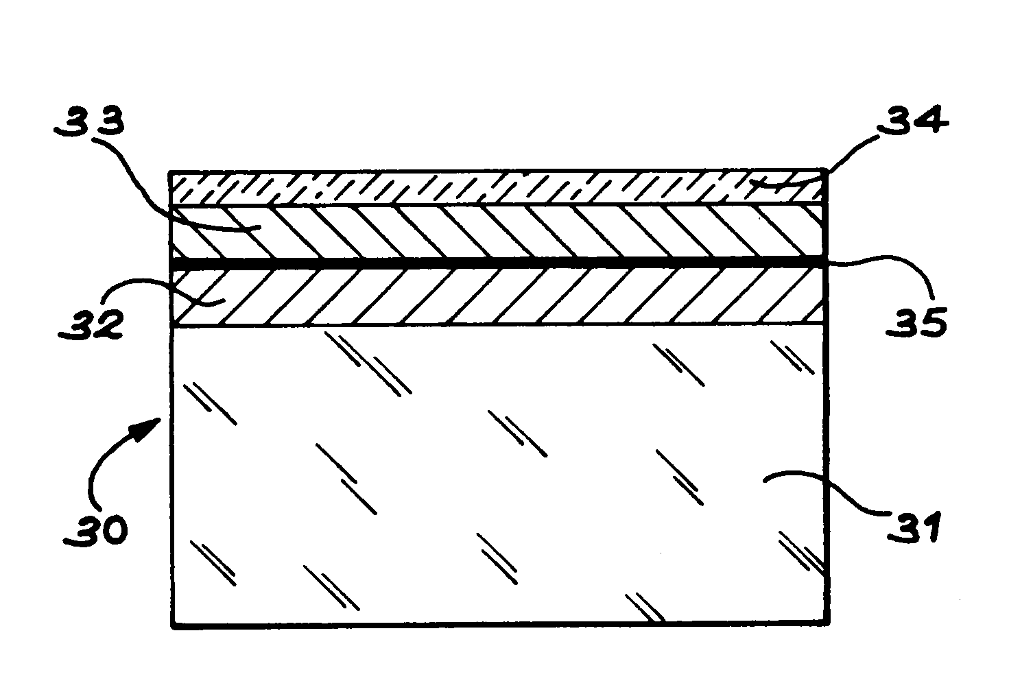
[0019]In order to remedy the disadvantages of the prior art, the present invention puts forward a compliant substrate which offers a thin layer of a material intended to be used to germinate hetero-epitaxial growth of another material. This thin layer is joined to the remainder of the substrate by joining means, which may be termed an embedded region, such that the thin layer and / or joining means accommodate all or part of the stresses caused during epitaxial growth of the epitaxied material, thereby preventing the occurrence of these stresses in the epitaxied material.

Problems solved by technology

However, at the present time it is only known how to fabricate solid substrates for certain semiconductors such as silicon, gallium arsenide, silicon carbide and indium phosphide for example.
However, this constraint of having to adapt lattice parameters at the interface of growth between layer and substrate severely limits the number and diversity of layers which may be grown, as it is only rarely possible to find a substrate whose network is adapted to the desired layer.
The use of ill-adapted substrates leads to the growth of layers of very poor quality.
In particular, as soon as the thickness of the layer exceeds a critical value, which decreases the more the networks are ill-adapted, the stresses are released in the hetero-epitaxial layer through the creation of structure defects (dislocations in particular).
However, even using all this know-how, the materials obtained always contain crystalline defects and are frequently of insufficient quality to fabricate optoelectronic and / or electronic devices.
One first group relates to a very fine substrate (a few nm) that is self-supporting, which is very difficult to produce and even virtually impossible if it is required to obtain large surface areas.
In this case, the superficial film obtained is very thin and the underlying insulator layer is likely to undergo deformation under the effect of the temperature during growth of the thin film.
These compliant substrates of the prior art have certain limitations in use.
For the self-supporting film, the limitation resides in the difficulty or virtual impossibility to produce a film of a few nm on a surface of several mm2, and even more so, several dozen cm2.
No material exists at these thicknesses that is sufficiently rigid for handling.
For the SOI structure, the limitation resides in the imperfect compliance of the substrate.
These heat treatments are not always compatible with the layer to be epitaxied.
For the third group of substrates, the difficulty is to obtain defect-free bonding over a large surface and to thin the layer down to a very narrow thickness.
. . ) of these defects may change during heat treatments, in particular these cavities may have their size increased.
Cavity size and the pressure within these cavities are not sufficient to induce surface deformation.
In this case, the cavities obtained are present even at annealing temperatures in the order of 1000° C. These defects cause strong, deep weaknesses in the material.

Method used


Image

  • Compliant Substrate In Particular For Hetero-Epitaxial Depositing
  • Compliant Substrate In Particular For Hetero-Epitaxial Depositing
  • Compliant Substrate In Particular For Hetero-Epitaxial Depositing

Examples


Embodiment Construction

[0035]By way of preferred example, the remainder of the description shall relate to the fabrication of compliant substrates for the depositing of materials by hetero-epitaxy.

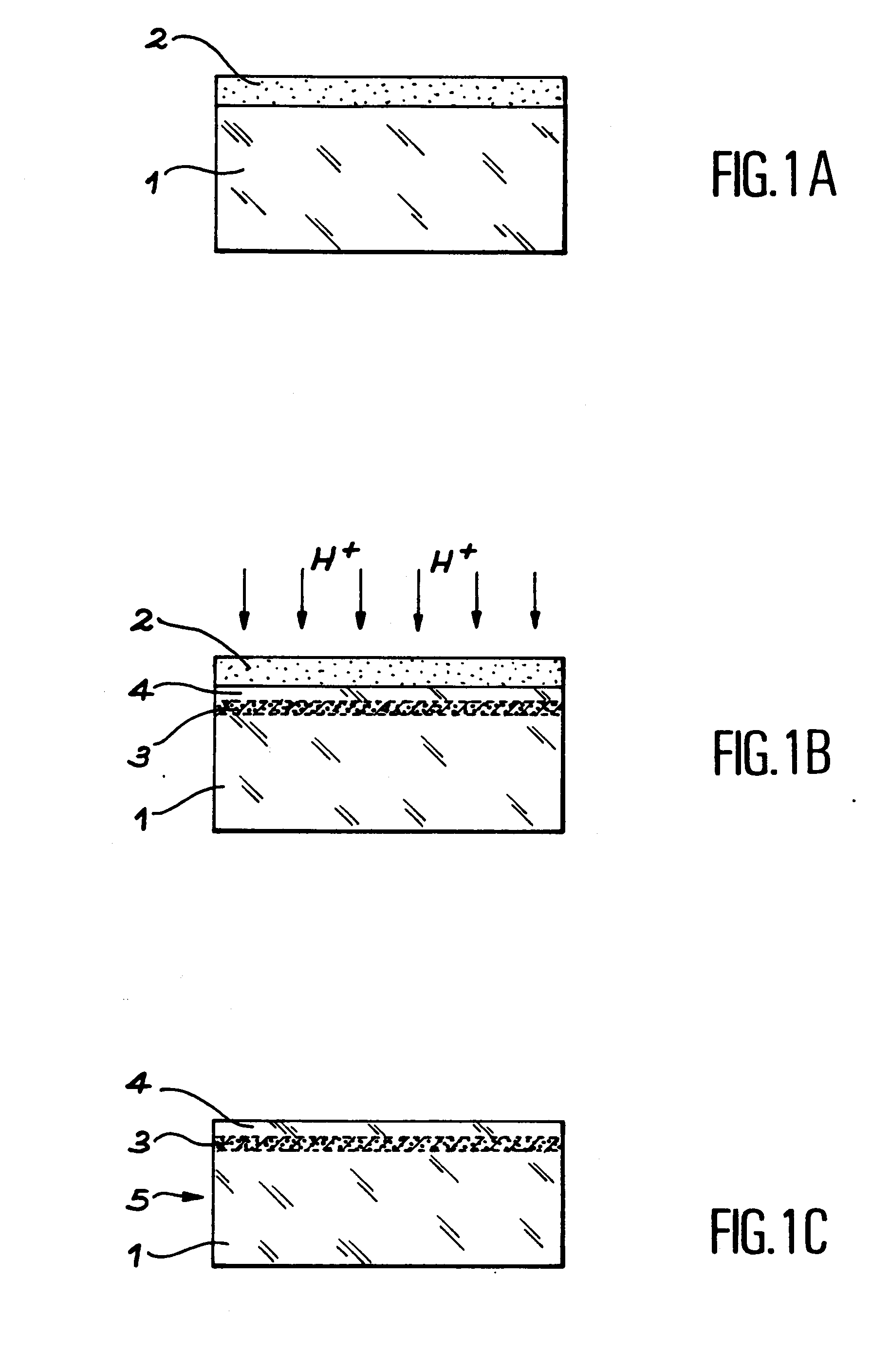
[0036]It is possible to obtain a film of narrow thickness from a substrate in which implantation of species is made (of ions for example) able to create, at a depth close to the average penetration depth of the species, a layer of defects which, between the substrate surface and itself, delimits a film of narrow thickness. The species are chosen such that the layer of created defects is able to accommodate the stresses to which the film of narrow thickness may be subjected. The role of the layer of defects is also to carry the film of narrow thickness (vertical action, perpendicular to the surface) while leaving it free of stresses in the horizontal plane (parallel to the surface). It may be necessary, in some cases, to apply heat treatment to the substrate after the implantation step so as for example to increa...


PUM

PropertyMeasurementUnit
Energyaaaaaaaaaa
Stress optical coefficientaaaaaaaaaa
Surface roughnessaaaaaaaaaa

Abstract

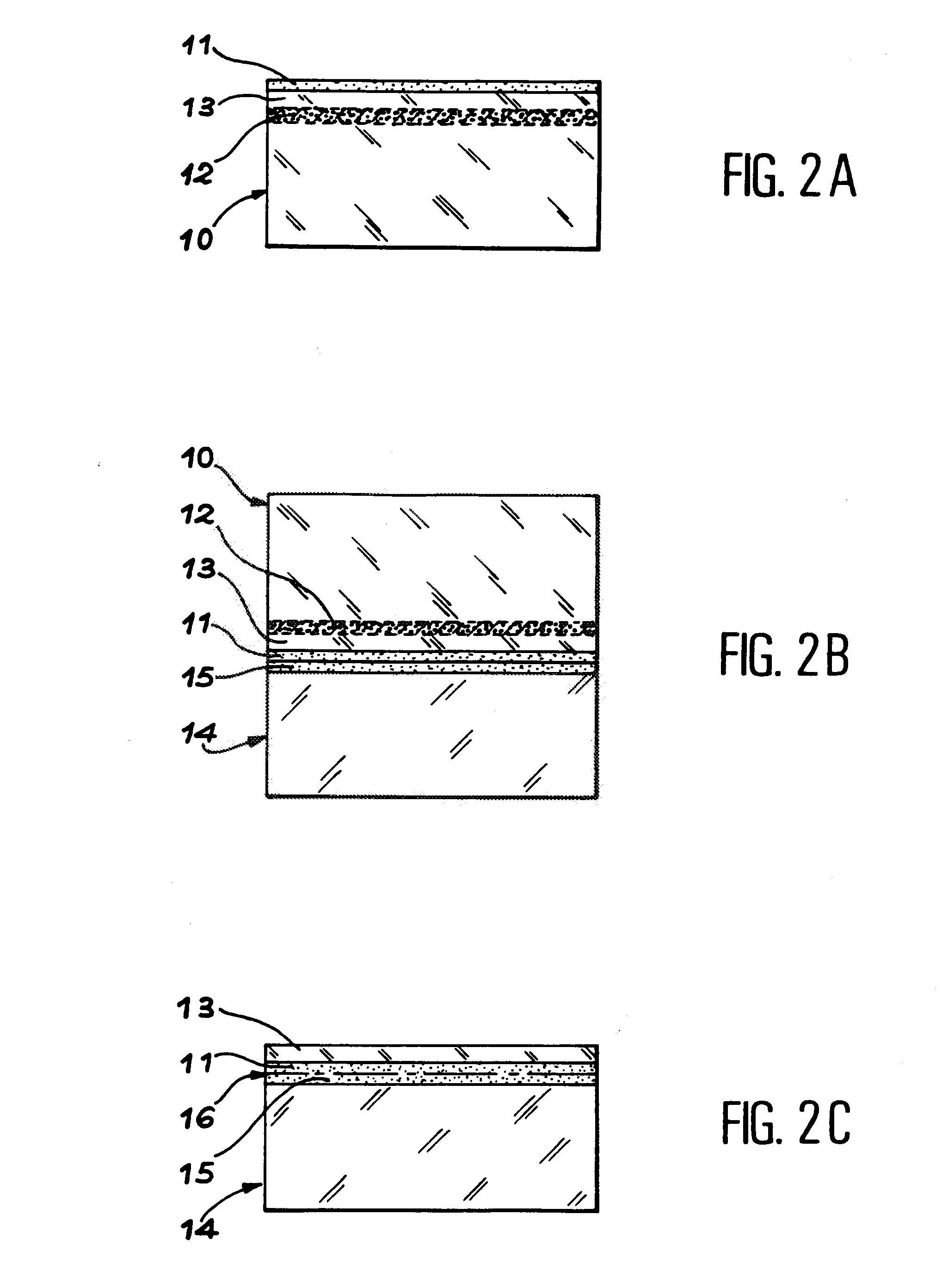
The invention relates to a compliant substrate (5) comprising a carrier (1) and at least one thin layer (4), formed on the surface of the carrier and intended to receive, in integral manner, a stress-giving structure. The carrier (1) and the thin layer (4) are joined to one another by joining means (3) such that the stresses brought by said structure are absorbed in whole or in part by the thin layer (4) and / or by the joining means (3) which comprise at least one joining zone chosen from among the following joining zones: a layer of microcavities and / or a bonding interface whose bonding energy is controlled to permit absorption of said stresses.

Description

TECHNICAL FIELD[0001]This invention relates to a compliant substrate, that is to say a substrate able to accept stresses induced by a structure adhering to it, and which may be a layer deposited on a surface of this substrate by hetero-epitaxy such that this layer suffers the least possible stress. It also relates to processes for obtaining such substrates.PRIOR ART[0002]Electronic and optoelelectronic applications demand a growing number of semiconductor materials and in particular compound semiconductors such as, for example, those of III-V type. However, at the present time it is only known how to fabricate solid substrates for certain semiconductors such as silicon, gallium arsenide, silicon carbide and indium phosphide for example. For other semiconductors, the solution chosen is hetero-epitaxial growth on a substrate whose crystalline network is adapted to that of the semiconductor layer which is to be grown.[0003]However, this constraint of having to adapt lattice parameters ...

Claims


Application Information

Patent Timeline
IPC IPC(8): B32B3/00B32B15/00H01L21/02H01L21/20H01L21/265H01L21/762H01L27/12
CPCH01L21/2007Y10T428/24355H01L21/76254Y10T428/31678
Inventor ASPAR, BERNARDBRUEL, MICHELJALAGUIER, ERICMORICEAU, HUBERT
Owner COMMISSARIAT A LENERGIE ATOMIQUE ET AUX ENERGIES ALTERNATIVES
Learn More