Prepreg, Method for Manufacturing Prepreg, Substrate, and Semiconductor Device
a semiconductor device and pre-preg technology, applied in the direction of solid-state devices, synthetic resin layered products, packaging, etc., can solve the problems of increasing the size and thickness of electronic devices, electronic parts, electronic devices and the like, and the difficulty of selecting a resin composition
- Summary
- Abstract
- Description
- Claims
- Application Information
AI Technical Summary
Benefits of technology
Problems solved by technology
Method used
Image

Examples
first embodiment
[0062]First, a preferred embodiment (first embodiment) of the prepreg according to the present invention will be described based on the accompanying drawings.
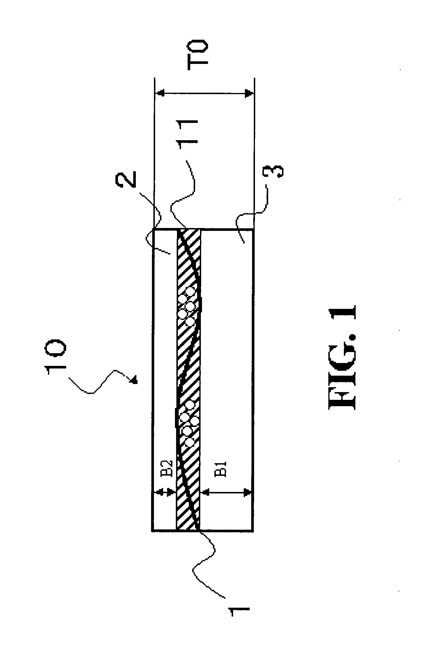
[0063]FIG. 1 is a sectional view showing one example (first embodiment) of the prepreg according to the present invention. In this regard, it is to be noted that, in the following description, the upper side and the lower side in FIG. 1 will be referred to as “upper side” and “lower side”, respectively (the same goes for other drawings).
[0064]A prepreg (that is, a resin film for forming a multilayer wiring substrate) 10 includes a core layer 11 having a sheet-shaped base member (that is, a fiber base member) 1, a first resin layer 2 provided on one surface of the core layer 11, and a second resin layer 3 provided on the other surface of the core layer 11.
[0065]The first resin layer 2 of the prepreg 10 is formed of a first resin composition, and the second resin layer 3 of the prepreg 10 is formed of a second resin composition. ...
second embodiment
[0306]Hereinbelow, another preferred embodiment (second embodiment) of the prepreg according to the present invention will be described based on the accompanying drawings.
[0307]In this regard, it is to be noted that the prepreg according to the second embodiment will be described by focusing differences between the first and second embodiments, and a description of the overlapping points will be omitted.
[0308]FIGS. 4(a), 4(b) and 5 are sectional views each showing one example (second embodiment) of the prepreg according to the present invention. In this regard, it is to be noted that a top and a bottom of each of FIGS. 4(a) and 4(b) are in a reversed relation with respect to those of FIG. 5.
[0309]A prepreg 10 according to the second embodiment is different from the prepreg 10 according to the first embodiment in the following points. Namely, in the prepreg 10 according to the second embodiment, a constitution of a first resin composition constituting a first resin layer 2 is identic...
example 1
1. Preparation of Varnish for Forming First Resin Layer
[0373]24 wt % of cyanate resin having a weight average molecular weight of about 2,600 (“Primaset PT-30” produced by LONZA Japan) as thermosetting resin, 24 wt % of biphenyldimethylene type epoxy resin having an epoxy equivalent of 275 (“NC-3000” produced by Nippon Kayaku Co., Ltd.) as epoxy resin, 11.8 wt % of phenoxy resin being a copolymer of bisphenol A type epoxy resin and bisphenol F type epoxy resin, having an epoxy group at each end, and having a weight average molecular weight of 60,000 (“EP-4275” produced by Japan Epoxy Resins Co., Ltd.) as phenoxy resin, and 0.2 wt % of an imidazole compound (“2-phenyl-4,5-dihydroxymethyl imidazole” produced by Shikoku Chemicals Corporation) as a curing catalyst were dissolved into methyl ethyl ketone to obtain a mixture.
[0374]Further, 39.8 wt % of spherical molten silica having an average particle size of 0.5 μm (“SO-25H” produced by Admatechs Co., Ltd.) as an inorganic filler and 0....
PUM
| Property | Measurement | Unit |
|---|---|---|
| thickness | aaaaa | aaaaa |
| peel strength | aaaaa | aaaaa |
| thickness | aaaaa | aaaaa |
Abstract
Description
Claims
Application Information
 - R&D
- Intellectual Property
- Life Sciences
- Materials
- Tech Scout
- Unparalleled Data Quality
- Higher Quality Content
- 60% Fewer Hallucinations
Browse by: Latest US Patents, China's latest patents, Technical Efficacy Thesaurus, Application Domain, Technology Topic, Popular Technical Reports.
© 2025 PatSnap. All rights reserved.Legal|Privacy policy|Modern Slavery Act Transparency Statement|Sitemap|About US| Contact US: help@patsnap.com