
Phase change memory device having a word line contact and method for manufacturing the same

a memory device and word line technology, applied in semiconductor devices, semiconductor/solid-state device details, electrical equipment, etc., can solve the problems of high operation voltage relative to power supply voltage, difficult to achieve a high level of integration, and difficult to achieve high level of integration

Active Publication Date: 2009-12-10
SK HYNIX INC
View PDF1 Cites 20 Cited by
  • Summary
  • Abstract
  • Description
  • Claims
  • Application Information

AI Technical Summary

Benefits of technology

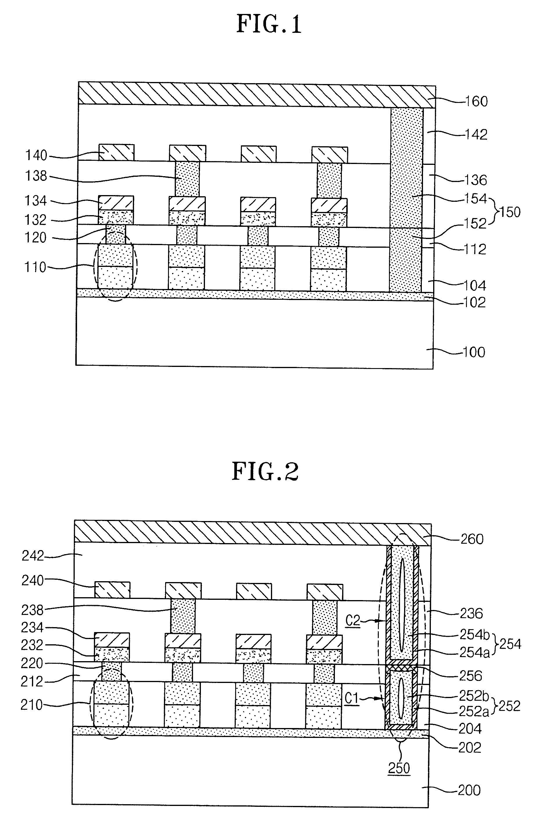
[0016]Embodiments of the present invention are directed to a phase change memory device in which a word line contact for connecting a word line to an N+ base layer can be formed in a stable manner and a method for manufacturing the same.
[0017]Additionally, embodiments of the present invention are directed to a phase change memory device in which a word line contact is formed in a stable manner allowing for uniform contact resistance between a word line and an N+ base layer, and a method for manufacturing the same.
[0018]Further, embodiments of the present invention are directed to a phase change memory device in which the contact resistance between a word line and an N+ base layer is uniform, thereby ensuring a stable current flow between a cell switching element and the word line, and a method for manufacturing the same.

Problems solved by technology

In order to obtain a high charge storing capacity, the surface area of certain electrodes in the DRAM must be increased; however, if the surface area of the electrodes is increased it is difficult to achieve a high level of integration.
Further, in a flash memory device two gates are stacked on each other, and thus a high operation voltage relative to a power supply voltage is required.
Therefore, a separate booster circuit is necessary in order to generate the voltage necessary for write and delete operations, which in turn makes it difficult to achieve a high level of integration.
However, the above-described conventional phase change memory device is not without problems as is described below.
Specifically, when etch loss of the first contact plug 152 is substantial, the N+ base layer 102 may also be etched causing damage to the N+ base layer 102, and thus the reliability of the phase change memory device can be seriously deteriorated.

Method used


Image

  • Phase change memory device having a word line contact and method for manufacturing the same
  • Phase change memory device having a word line contact and method for manufacturing the same
  • Phase change memory device having a word line contact and method for manufacturing the same

Examples


Embodiment Construction

[0050]Hereafter, specific embodiments of the present invention will be described with reference to the attached drawings.

[0051]FIG. 2 is a cross-sectional view showing a phase change memory device according to an embodiment of the present invention.

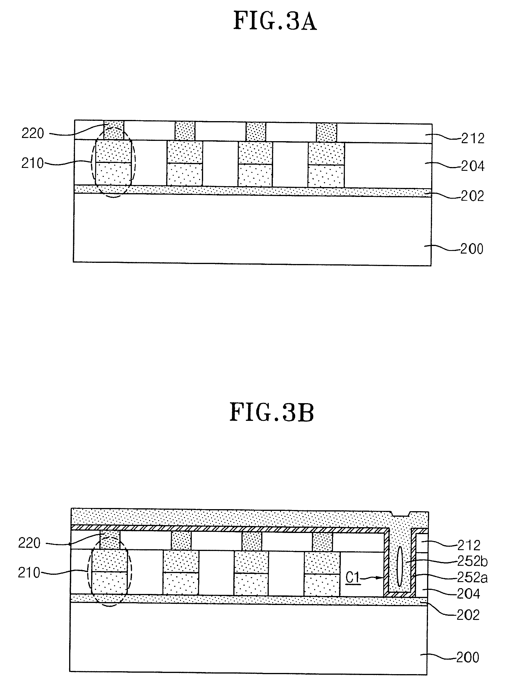
[0052]Referring to FIG. 2, a plurality of cell switching elements 210 comprising vertical PN diodes are formed on a semiconductor substrate 200. The semiconductor substrate 200 includes a plurality of bar-type active regions extending in a first direction and separated from each other by regular intervals extending in a second direction perpendicular to the first direction. Each of the cell switching elements 210 comprises a stack pattern of an N-type silicon layer and a P-type silicon layer to form a vertical PN diode. A predetermined number of cell switching elements 210 comprising the vertical PN diodes (for example, a multiple of 2) constitute one string.

[0053]An N+ base layer 202 is formed in a surface of the semiconductor substrate ...


PUM


Abstract

A phase change memory device having a word line contact includes an N+ base layer formed in a surface of a semiconductor substrate. A word line is formed over the N+ base layer. The word line contact is formed to connect the N+ base layer to the word line. The word line contact includes a first contact plug, a barrier layer formed on the first contact plug, and a second contact plug formed on the barrier layer coaxially with the first contact plug. The barrier layer prevents unwanted etching of the first contact plug when the second contact plug is being formed.

Description

CROSS-REFERENCE TO RELATED APPLICATIONS[0001]The present application claims priority to Korean patent application number 10-2008-0052887 filed on Jun. 5, 2008, which is incorporated herein by reference in its entirety.BACKGROUND OF THE INVENTION[0002]The present invention relates generally to a phase change memory device and a method for manufacturing the same, and more particularly, to a phase change memory device in which a word line contact for connecting a word line to an N+ base layer can be stably formed and a method for manufacturing the same.[0003]Memory devices are typically grouped into volatile random access memory (RAM), in which data is lost when power is interrupted, and non-volatile read-only memory (ROM), in which stored data is maintained even when power is interrupted. Examples of volatile RAM include dynamic RAM (DRAM) and static RAM (SRAM), and examples of non-volatile ROM include flash memory devices such as electrically erasable and programmable ROM (EEPROM).[0...

Claims


Application Information

Patent Timeline
IPC IPC(8): H01L45/00H01L21/44
CPCH01L21/76849H01L21/76883H01L23/5226H01L27/2409H01L27/2463H01L45/06H01L2924/0002H01L45/1233H01L45/126H01L2924/00H10B63/20H10B63/80H10N70/231H10N70/826H10N70/8413H01L21/76897
Inventor CHANG, HEON YONG
Owner SK HYNIX INC
Learn More