Solar cell having a high quality rear surface spin-on dielectric layer
a solar cell and dielectric layer technology, applied in the field of solar cells, can solve the problems of contaminating silicon wafers, increasing manufacturing costs, and increasing operations, and achieve the effect of increasing manufacturing costs and increasing the number of operations
- Summary
- Abstract
- Description
- Claims
- Application Information
AI Technical Summary
Benefits of technology
Problems solved by technology
Method used
Image
Examples
Embodiment Construction
[0018]In the following detailed description, numerous specific details are set forth in order to provide a thorough understanding of the invention. However, it will be understood by those skilled in the art that the present invention may be practiced without these specific details. In other instances, well-known methods, procedures, components, and circuits have not been described in detail so as not to obscure the present invention.
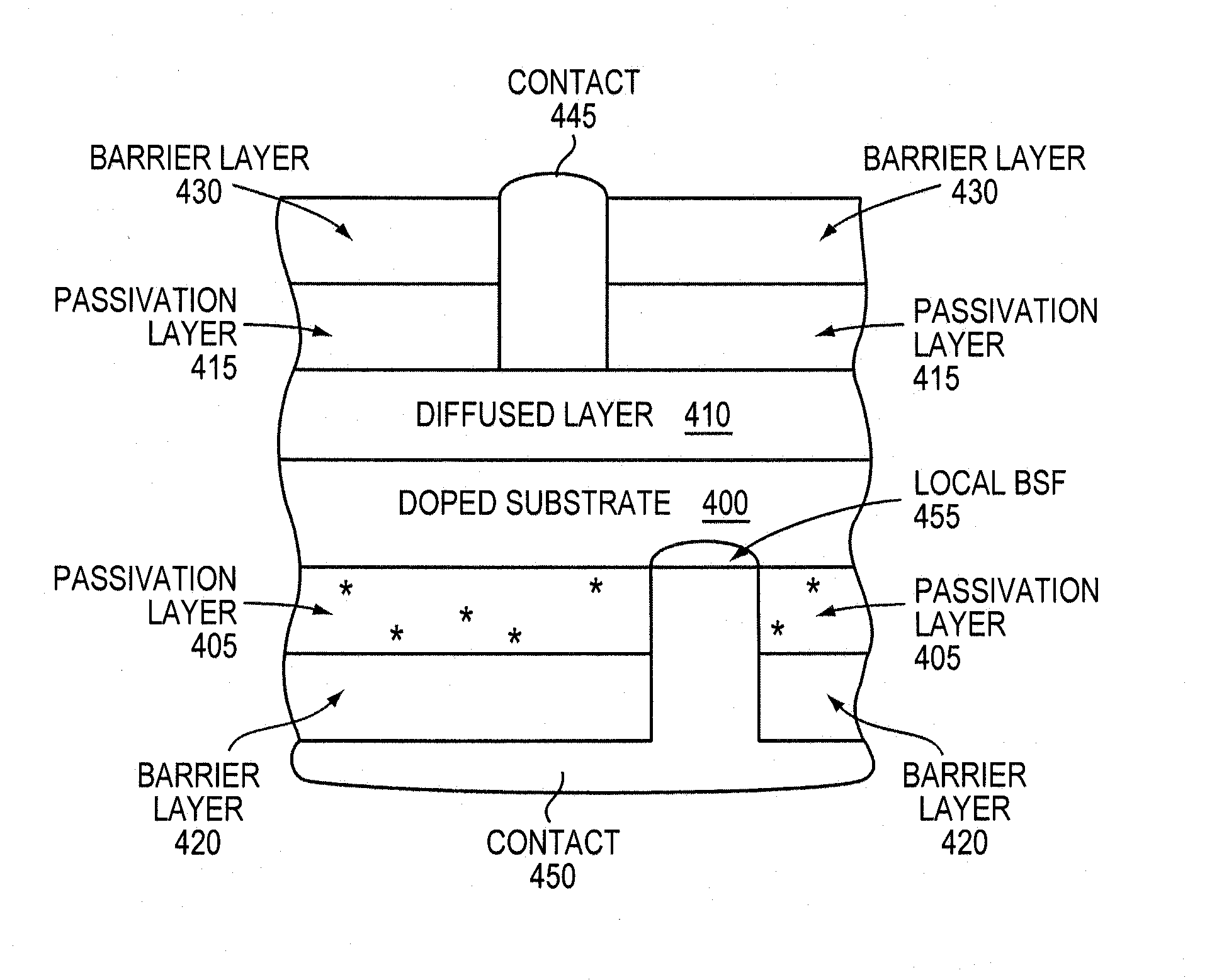
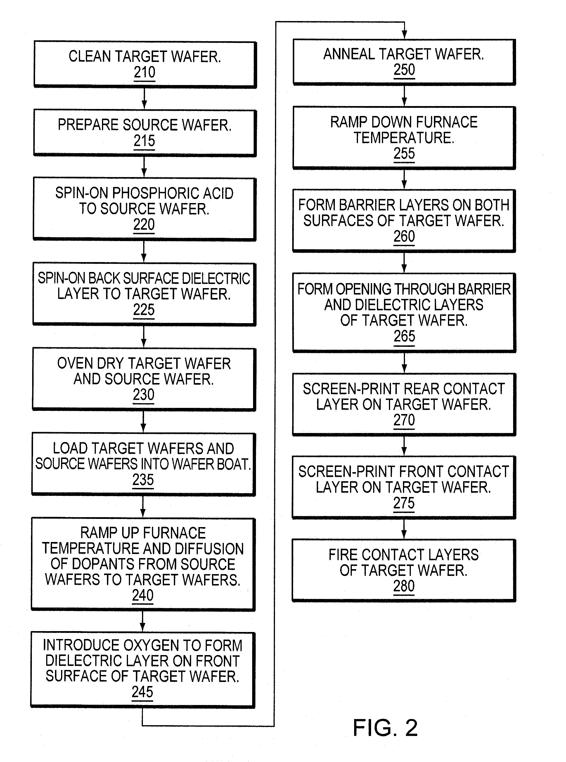
[0019]FIG. 2 is a flowchart for one embodiment of a process for creating simultaneous emitter diffusion and front and rear surface passivation. To minimize handling of cell wafers, this process involves a single diffusion and oxidation furnace operation. The process starts with silicon wafers, one of which is used as a dopant source wafer and the other of which is a target wafer on which the solar cell is to be formed. The target wafers may be Czochralski or Float Zone wafers. The target wafers may have a thickness from 50 to 500 micrometers. The target ...
PUM
 Abstract
Description
Claims
Application Information
 - R&D
- Intellectual Property
- Life Sciences
- Materials
- Tech Scout
- Unparalleled Data Quality
- Higher Quality Content
- 60% Fewer Hallucinations
Browse by: Latest US Patents, China's latest patents, Technical Efficacy Thesaurus, Application Domain, Technology Topic, Popular Technical Reports.
© 2025 PatSnap. All rights reserved.Legal|Privacy policy|Modern Slavery Act Transparency Statement|Sitemap|About US| Contact US: help@patsnap.com


