Bonding method for through-silicon-via based 3D wafer stacking
- Summary
- Abstract
- Description
- Claims
- Application Information
AI Technical Summary
Problems solved by technology
Method used
Image
Examples
Embodiment Construction
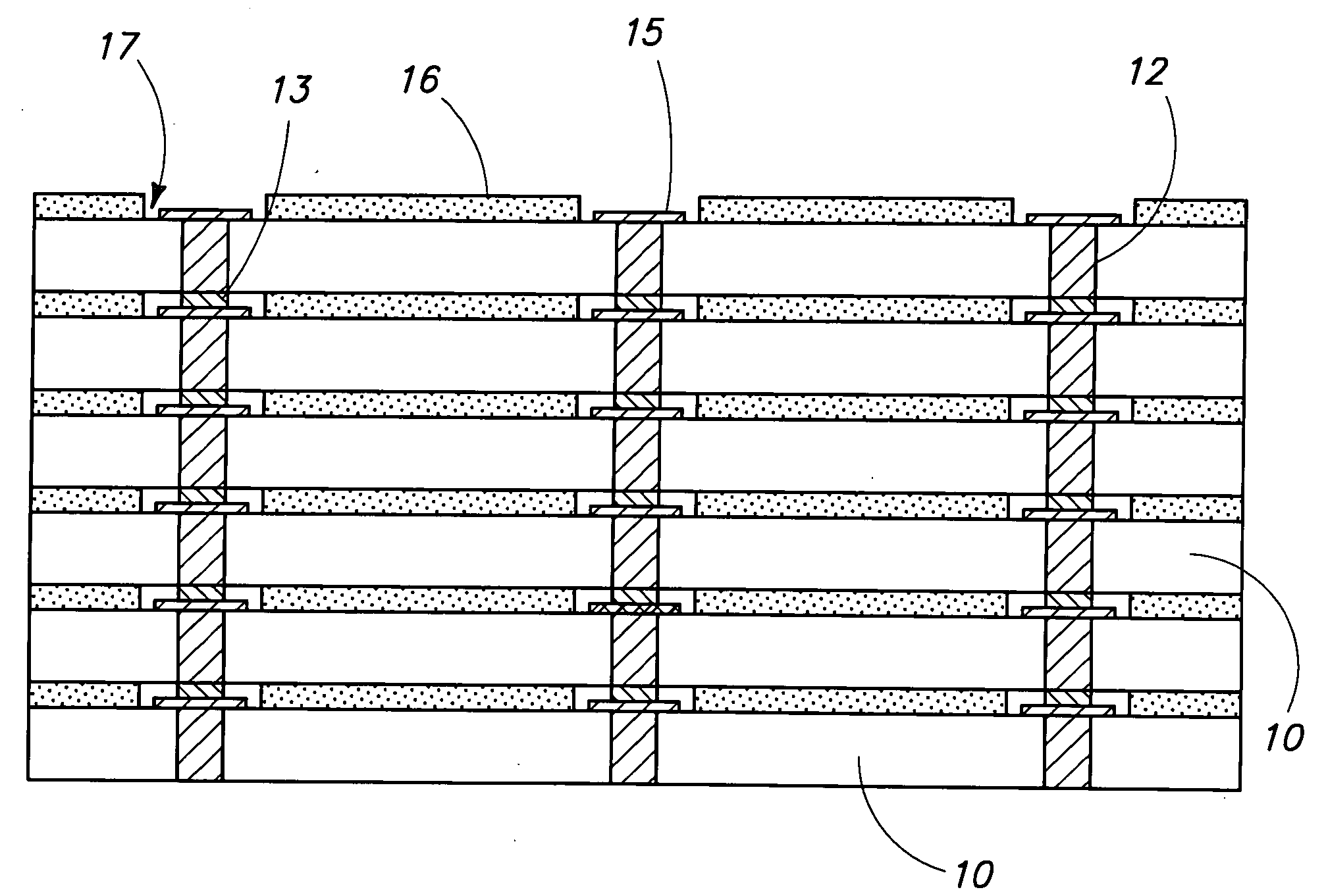
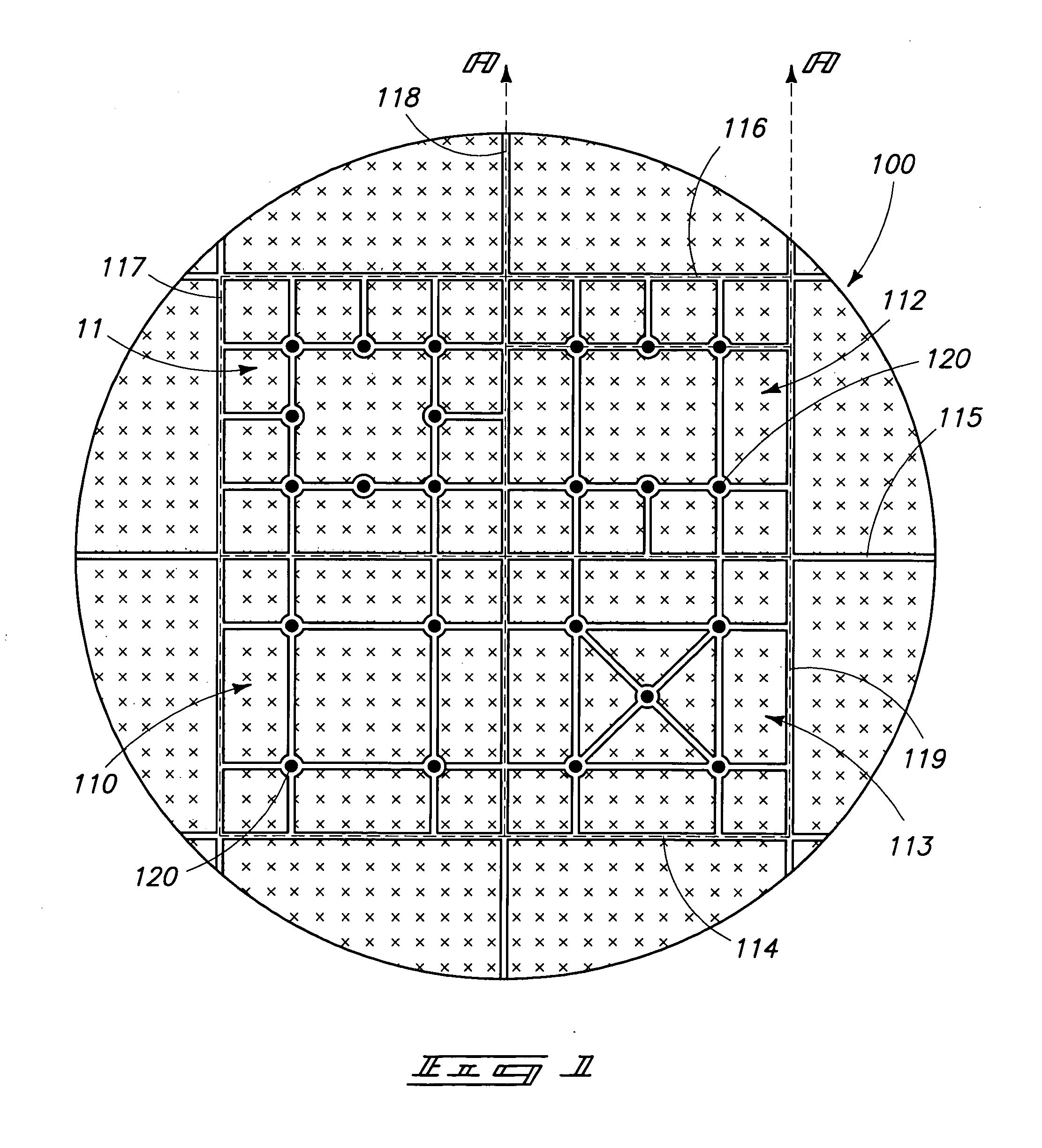
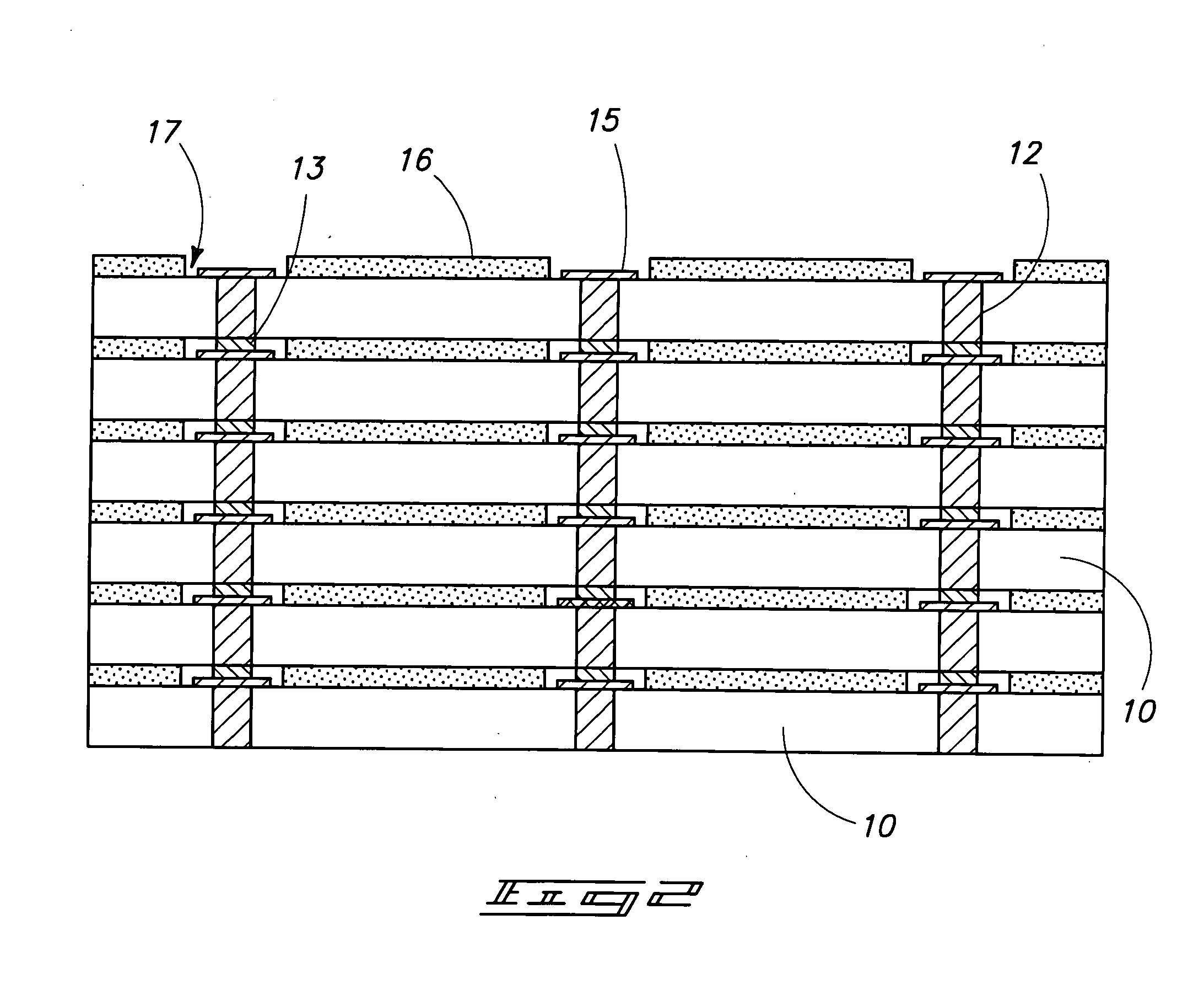
[0024]FIG. 1 shows an embodiment of the invention in the form of a circular wafer stack 100 which may be divided into four chips 110-113. FIG. 2 is a cross-sectional view along line A-A showing the structure of the wafer stack with a plurality of TSVs electrically connected by solder and with individual wafers bonded together by layers of adhesive that are patterned in a manner to be described below.
[0025]In this example each chip 110-113 has a different arrangement of vias 120 (e.g., a simple square in 110, two rows of three vias in 11 and 112, and a square with a central via in chip 113), but in each case every via is formed with a surrounding space that connects to an edge of the chip through channels either directly or through another surrounding space. It will be seen that the four chips are divided by mutually perpendicular main rows 114-119 that are channels formed by patterning the adhesive and which lead to the edge of the wafer. Each channel in one of the chips 110-113 ult...
PUM
 Abstract
Description
Claims
Application Information
 - R&D
- Intellectual Property
- Life Sciences
- Materials
- Tech Scout
- Unparalleled Data Quality
- Higher Quality Content
- 60% Fewer Hallucinations
Browse by: Latest US Patents, China's latest patents, Technical Efficacy Thesaurus, Application Domain, Technology Topic, Popular Technical Reports.
© 2025 PatSnap. All rights reserved.Legal|Privacy policy|Modern Slavery Act Transparency Statement|Sitemap|About US| Contact US: help@patsnap.com


