Method of manufacturing a printed circuit board

Active Publication Date: 2009-12-03
GM GLOBAL TECH OPERATIONS LLC +1
View PDF24 Cites 32 Cited by
  • Summary
  • Abstract
  • Description
  • Claims
  • Application Information

AI Technical Summary

Benefits of technology

[0010]The PCB produced by implementation of the method of the subject invention is durable, easily manufactured, and does not require time-consuming rework. Furthermore, the PCB provides substantially even surfaces, which reduces soldering defects of electronic components having numerous pins. Moreover, the PCB provides excellent heat transfer from one surface to another which reduces overheating of electrical and electronic components.

Problems solved by technology

Over the last several decades, these PCBs have become increasingly complex to match the complexity of the circuits they facilitate as well as aggressive size and packaging requirements.
Via in pad designs are often wrought with difficulties.
Another difficulty is the contamination of un-plugged via holes with conformal coatings used to protect the surfaces of the PCB.
This contamination degrades heat transfer and touch-up operations are often required to remove the conformal coating from the vias.
HASL finishes themselves often provide additional difficulties in PCB circuit operation.
This leads to less efficient thermal transfer.
Also, the HASL finish often presents an uneven surface which contributes to soldering defects, particularly with components having a large number of pins, such as a digital signal processor.

Method used


Image

  • Method of manufacturing a printed circuit board
  • Method of manufacturing a printed circuit board
  • Method of manufacturing a printed circuit board

Examples


Embodiment Construction

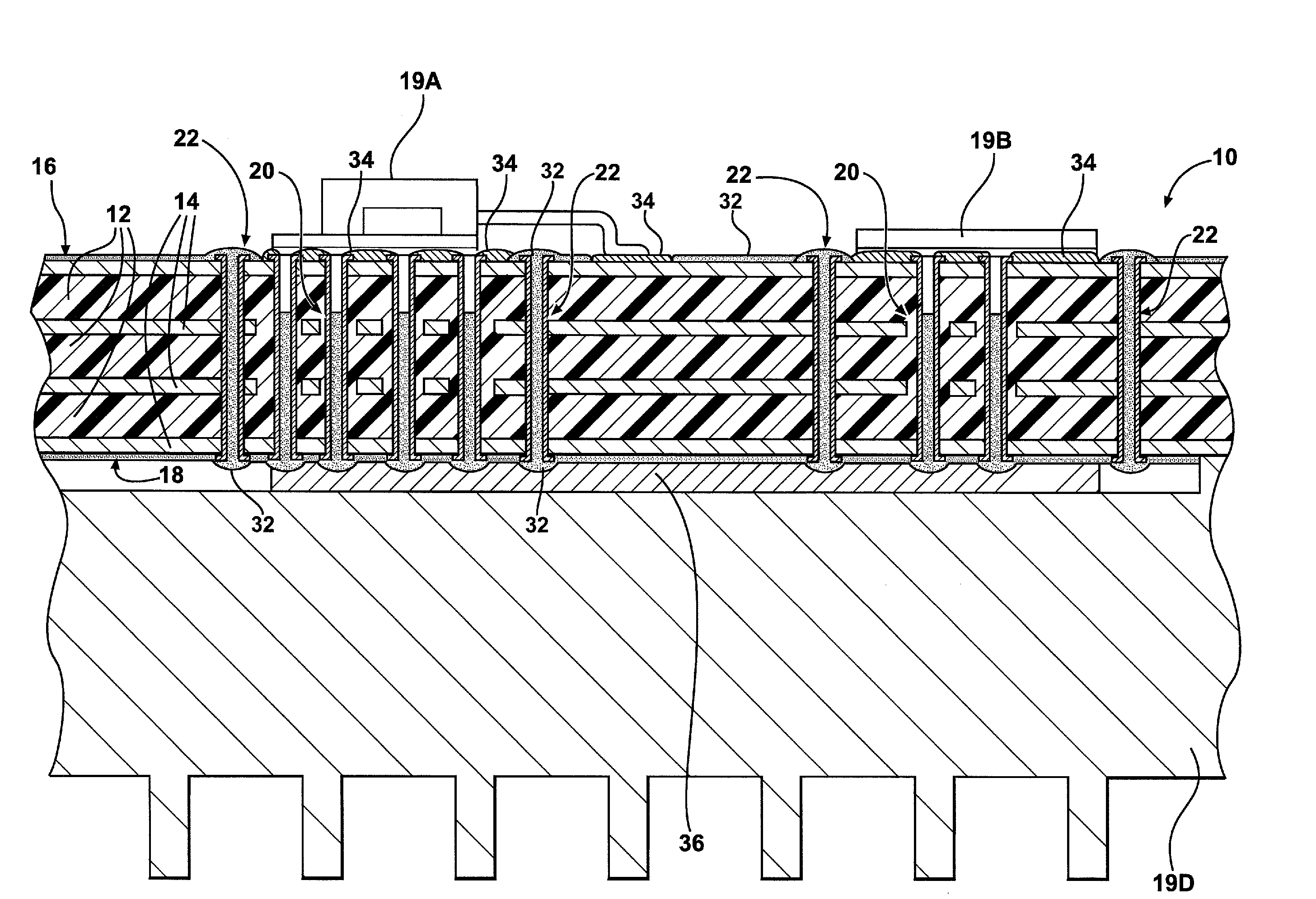
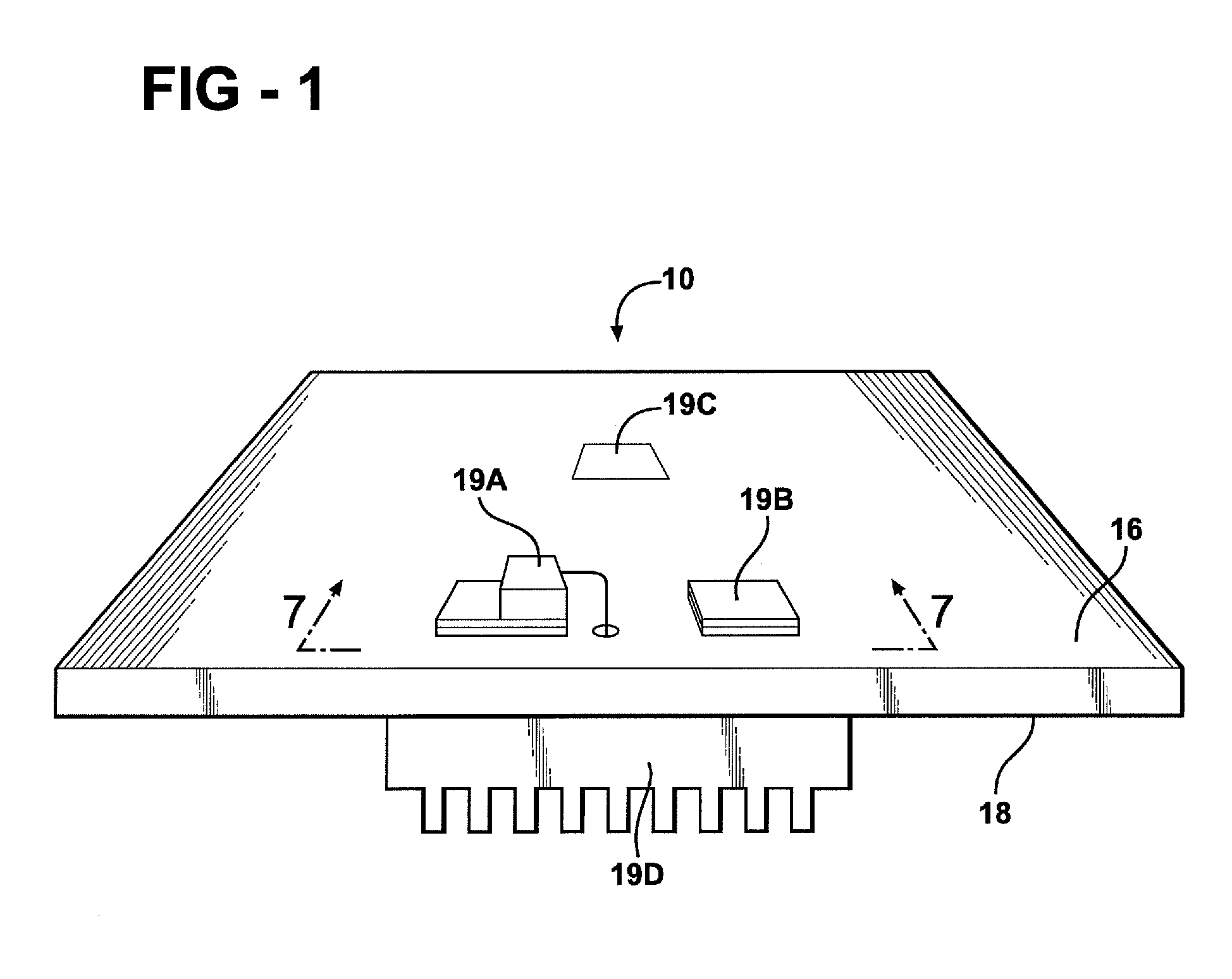
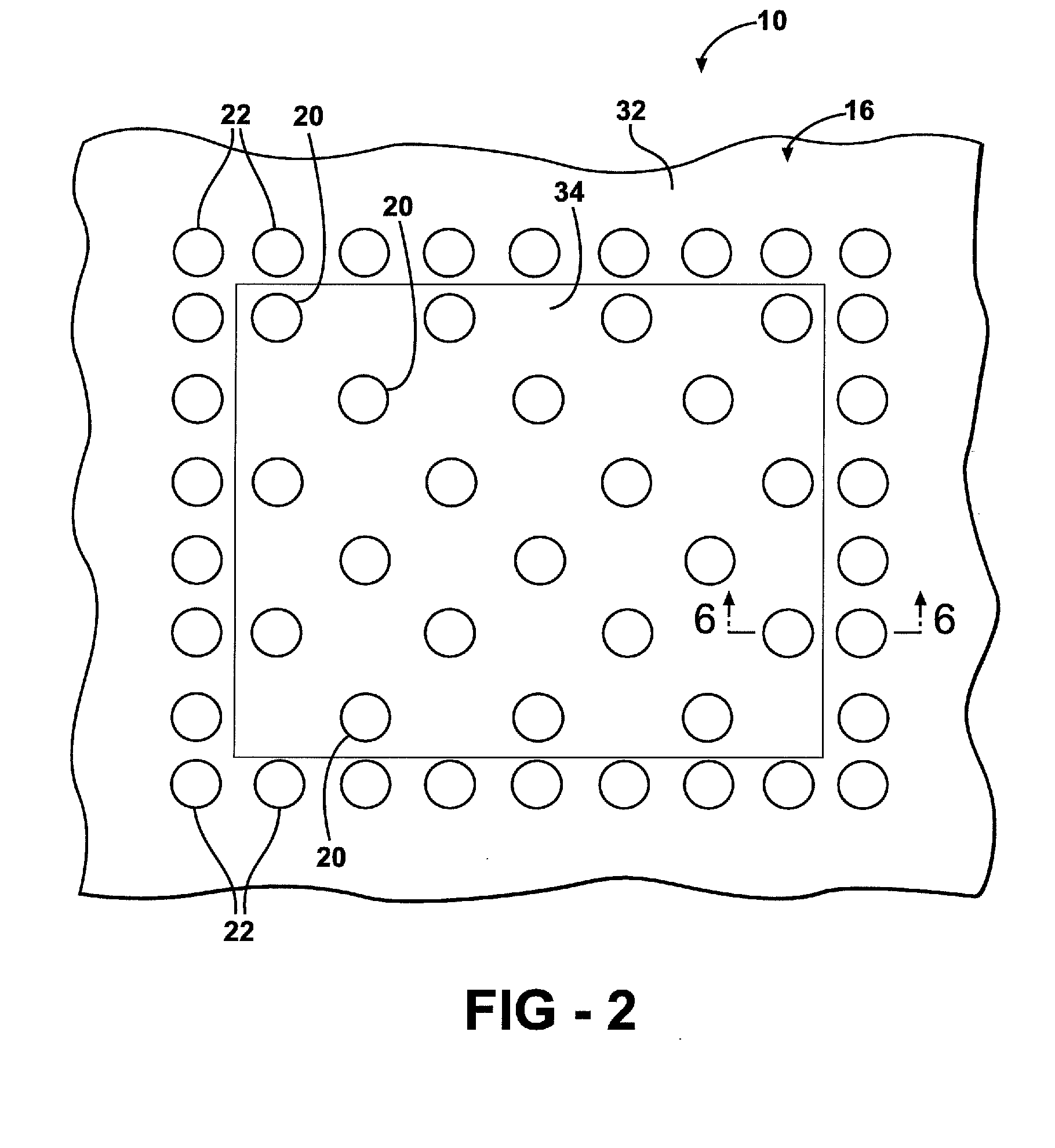
[0019]The subject invention provides a method of manufacturing a printed circuit board (PCB) 10. The PCB 10 is preferably a laminate of at least one non-conductive layer 12 and at least one conductive layer 14. The layers 12, 14 of the PCB 10 form a first surface 16 and a second surface 18. Various electrical and electronic components 19 are mountable and / or solderable to these surfaces 16, 18 as is well known to those skilled in the art.

[0020]The PCB 10 of the illustrated embodiment supports and electrically connects the various components 19 of an electronic power steering (EPS) controller (not numbered) for a vehicle (not shown). Of course, the teachings described herein are not limited to the particular application shown in the illustrated embodiment. That is, the PCB 10 may be utilized to electrically connect any number of components for any number of applications. The components 19 of the EPS controller, as shown in FIG. 1, include, but are not limited to, a MOSFET 19A, a curr...


PUM

PropertyMeasurementUnit
Fractionaaaaaaaaaa
Fractionaaaaaaaaaa
Fractionaaaaaaaaaa

Abstract

A method of manufacturing a printed circuit board (PCB) includes of disposing thermal transfer vias and electrical vias through the PCB. The method further includes filling holes of the vias with a solder mask. The thermal transfer vias are filled to about 70% of capacity while the electrical vias are completely filled. Once filled, surfaces of the PCB are coated with an organic solderability preservative.

Description

BACKGROUND OF THE INVENTION[0001]1. Field of the Invention[0002]The subject invention relates to a method of manufacturing a printed circuit board (PCB). Specifically, the subject invention relates to manufacturing a PCB having vias disposed through solder pads.[0003]2. Description of the Related Art[0004]Printed circuit boards (PCBs) are commonly used to support and electrically connect various components of an electrical or electronic circuit. Over the last several decades, these PCBs have become increasingly complex to match the complexity of the circuits they facilitate as well as aggressive size and packaging requirements.[0005]A typical modern PCB now utilizes a plurality of conductive layers separated by non-conductive layers. Interconnection between the conductive layers is often provided utilizing a plated-through hole, commonly known as a via. These vias provide electrical and thermal transfer from one side of the PCB to another. A recent trend in the manufacture of PCBs i...

Claims


Application Information

Patent Timeline
IPC IPC(8): H01R12/04H01K3/10
CPCH05K1/0206H05K1/0207H05K3/0094H05K3/282H05K3/3452Y10T29/49144H05K2201/09309H05K2201/0959H05K2201/10166Y10T29/49165H05K3/429
Inventor THOMAS, WAYNE BERNARD
Owner GM GLOBAL TECH OPERATIONS LLC
Why Eureka
Try Eureka