Semiconductor memory device
- Summary
- Abstract
- Description
- Claims
- Application Information
AI Technical Summary
Problems solved by technology
Method used
Image

Examples
first embodiment
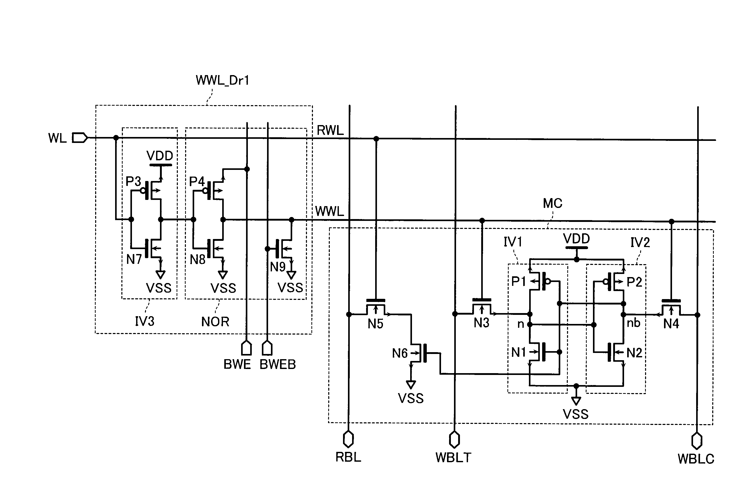
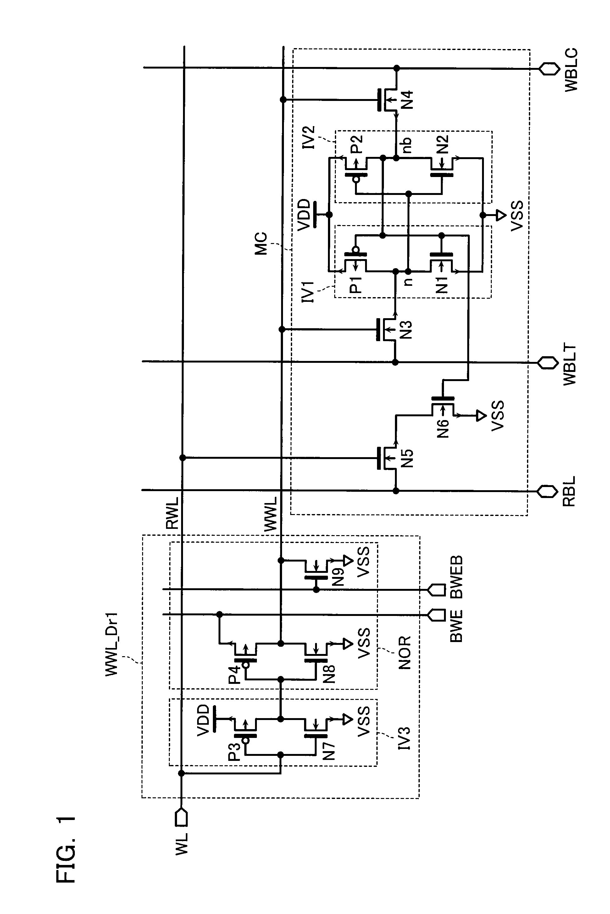
[0023]FIG. 1 is a circuit diagram of a memory cell and a word line driver in a semiconductor memory device according to a first embodiment of the present invention.
[0024]The semiconductor memory device according to the present embodiment comprises a read word line RWL provided in the row direction; a write word line WWL provided in parallel with the read word line RWL and split into several; and a read bit line RBL and a write bit line pair WBL composed of a first WBTL and a second write bit line WBLC provided in the column direction crossing the read word line RWL and the write word line WWL. Connected at an intersection of the read word line RWL and write word line WWL and the read bit line RBL and write bit line pair WBL is one of plural memory cells MC having a read port and a write port provided independently. The write word line WWL has one end provided with a word line driver WWL_Dr1 for driving the write word line WWL.
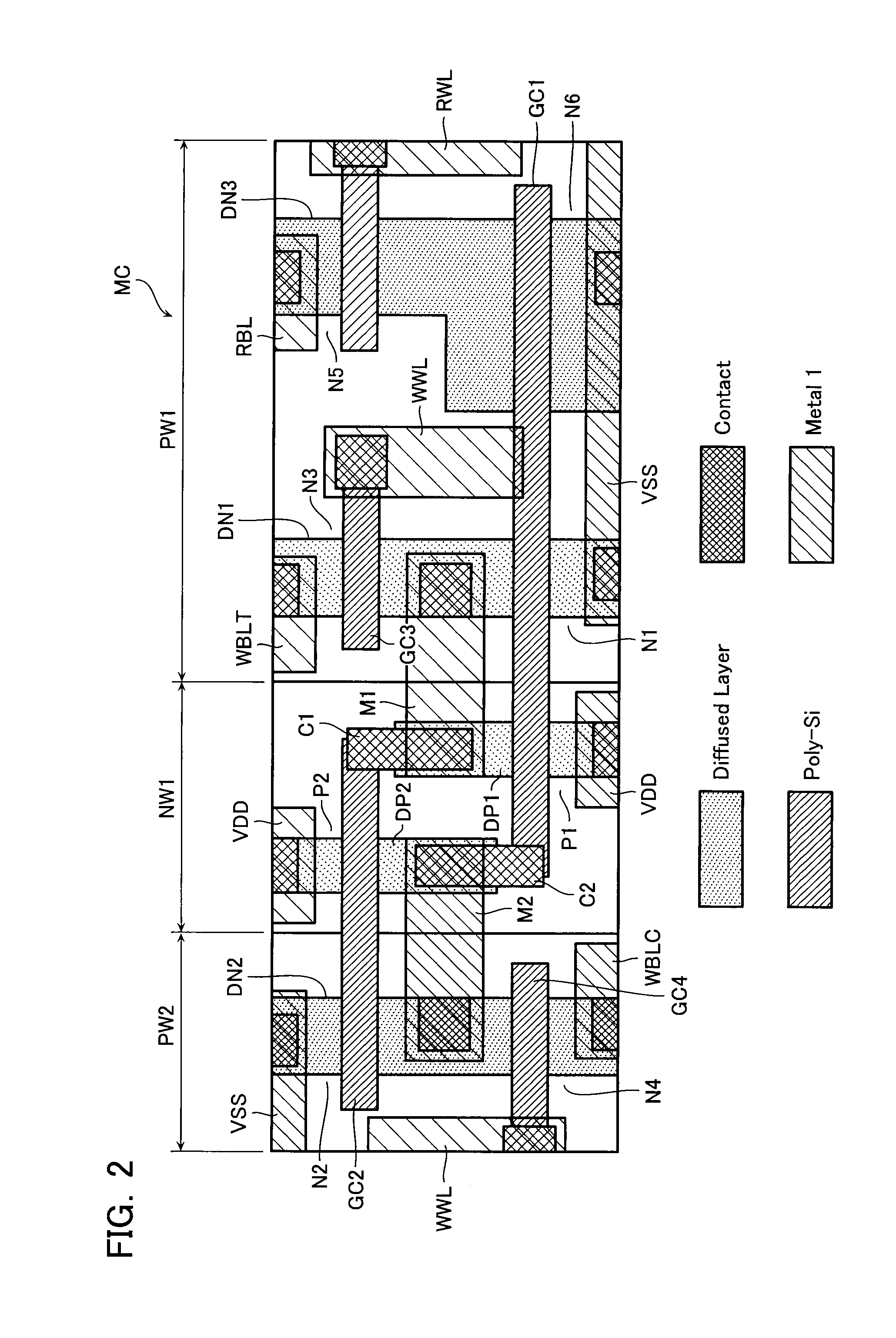
[0025]The memory cell MC is a memory cell of the 8-transi...
second embodiment
[0050]FIG. 6 is a circuit diagram of a memory cell and a word line driver in a semiconductor memory device according to a second embodiment of the present invention.
[0051]The semiconductor memory device according to the present embodiment comprises a word line driver WWL_Dr2 including a transfer gate in place of the word line driver WWL_Dr1 in the first embodiment.
[0052]The word line driver WWL_Dr2 includes a transfer gate TG having an input terminal connected to the read word line RWL and an output terminal connected to the write word line WWL, and a pull-down NMOS transistor N11 having a source connected to the ground line VSS, and a drain connected to the write word line WWL. The transfer transistor TG includes an NMOS transistor N10 and a PMOS transistor P5, of which sources and drains are mutually connected. The NMOS transistor N10 has a gate, which is connected to the first write enable signal line BWE. The PMOS transistor P5 and the NMOS transistor N11 have respective gates, ...
PUM
 Abstract
Description
Claims
Application Information
 - R&D
- Intellectual Property
- Life Sciences
- Materials
- Tech Scout
- Unparalleled Data Quality
- Higher Quality Content
- 60% Fewer Hallucinations
Browse by: Latest US Patents, China's latest patents, Technical Efficacy Thesaurus, Application Domain, Technology Topic, Popular Technical Reports.
© 2025 PatSnap. All rights reserved.Legal|Privacy policy|Modern Slavery Act Transparency Statement|Sitemap|About US| Contact US: help@patsnap.com