
Nonvolatile memory apparatus, nonvolatile memory element, and nonvolatile element array

a nonvolatile memory and array technology, applied in the direction of digital storage, instruments, semiconductor devices, etc., can solve the problems of varying the resistance value of the resistance variable memory element in the low-resistance state, the limitation of miniaturization of an existing flash memory using a floating gate, and the complex composition of perovskite materials, etc., to achieve high affinity with a semiconductor manufacturing process, high-speed operation, and stable rewriting characteristics

Active Publication Date: 2009-10-08
PANASONIC SEMICON SOLUTIONS CO LTD
View PDF15 Cites 56 Cited by
  • Summary
  • Abstract
  • Description
  • Claims
  • Application Information

AI Technical Summary

Benefits of technology

[0047]In accordance with the present invention, a nonvolatile memory apparatus, a nonvolatile memory element, and a nonvolatile memory element array which are capable of high-speed operation and have a stably reversible rewrite characteristic using a material which has high affinity with a semiconductor manufacturing process are attained.

Problems solved by technology

In response to such demands, it is said that there is a limitation on miniaturization of an existing flash memory using a floating gate.
However, the perovskite material has a complex composition and is not always compatible with a CMOS process.
However, a problem arises, in which, when amorphous rare earth metal is used as the variable resistance material, the resistance value of the resistance variable memory element in the low-resistance state varies if the low-resistance attaining pulse is applied thereto.

Method used


Image

  • Nonvolatile memory apparatus, nonvolatile memory element, and nonvolatile element array
  • Nonvolatile memory apparatus, nonvolatile memory element, and nonvolatile element array
  • Nonvolatile memory apparatus, nonvolatile memory element, and nonvolatile element array

Examples


embodiment 1

Configuration of Nonvolatile Memory Apparatus and Nonvolatile Memory Element

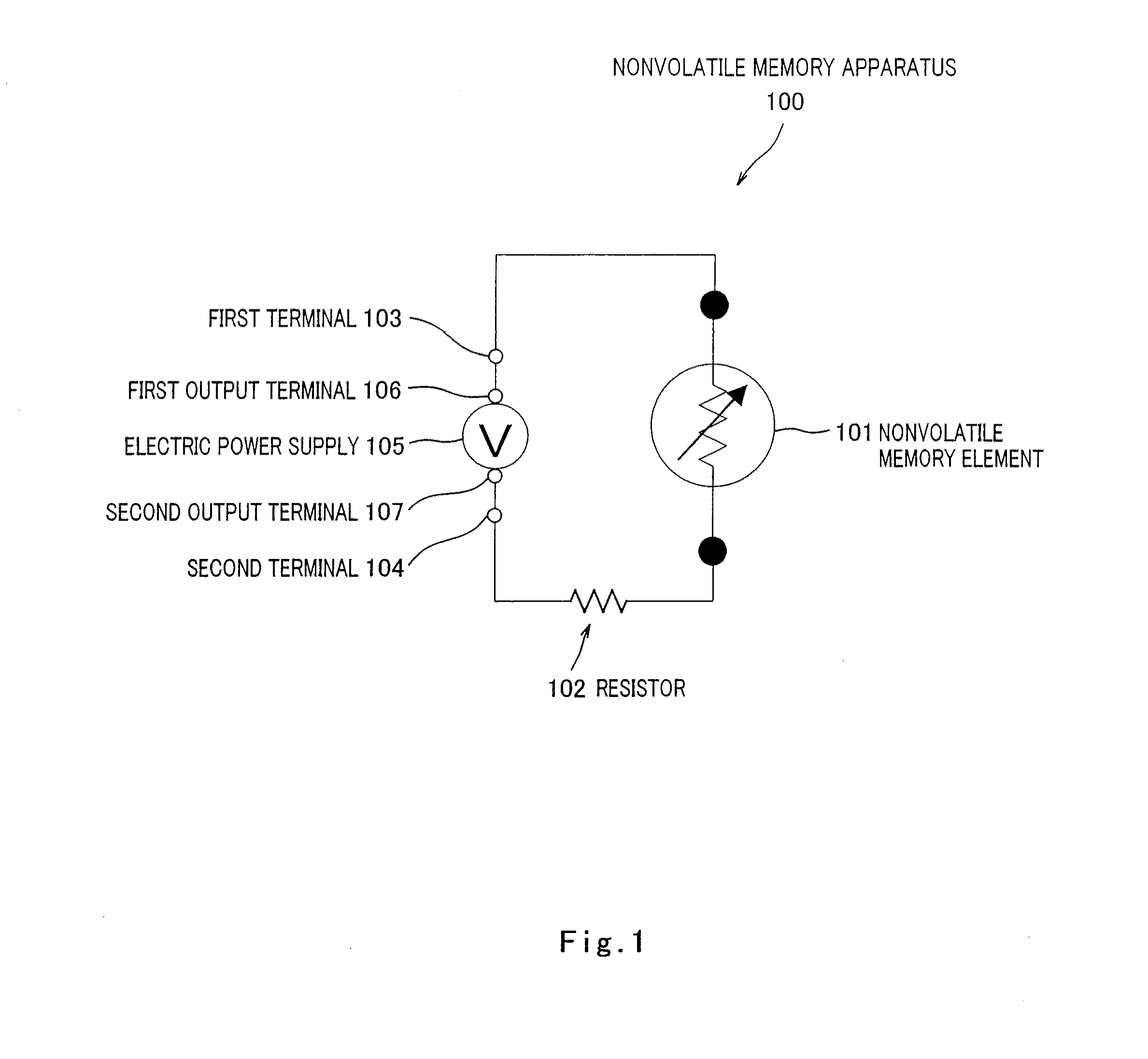
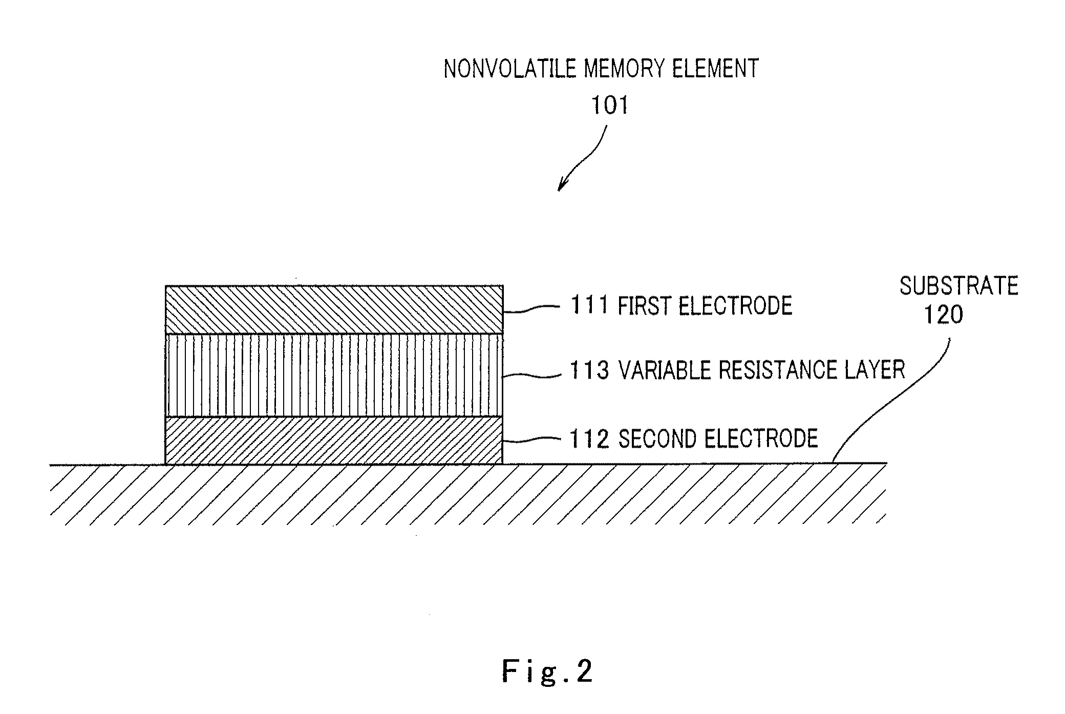
[0129]FIG. 1 is a circuit diagram showing an example of a configuration of a nonvolatile memory apparatus according to Embodiment 1 of the present invention. FIG. 2 is a cross-sectional view showing an example of the nonvolatile memory element of FIG. 1.

[0130]As shown in FIG. 1, a nonvolatile memory apparatus 100 of this embodiment includes a nonvolatile memory element 101, a resistor 102, a first terminal 103, and a second terminal 104.

[0131]As shown in FIG. 1, when the nonvolatile memory apparatus 100 is used, an electric power supply (electric pulse application unit) 105 is connected between the first terminal 103 and the second terminal 104. The electric power supply 105 has a first output terminal 106 and a second output terminal 107. The first output terminal 106 and the first terminal 103 are connected to each other. The second output terminal 107 and the second terminal are connected to each other. I...

example

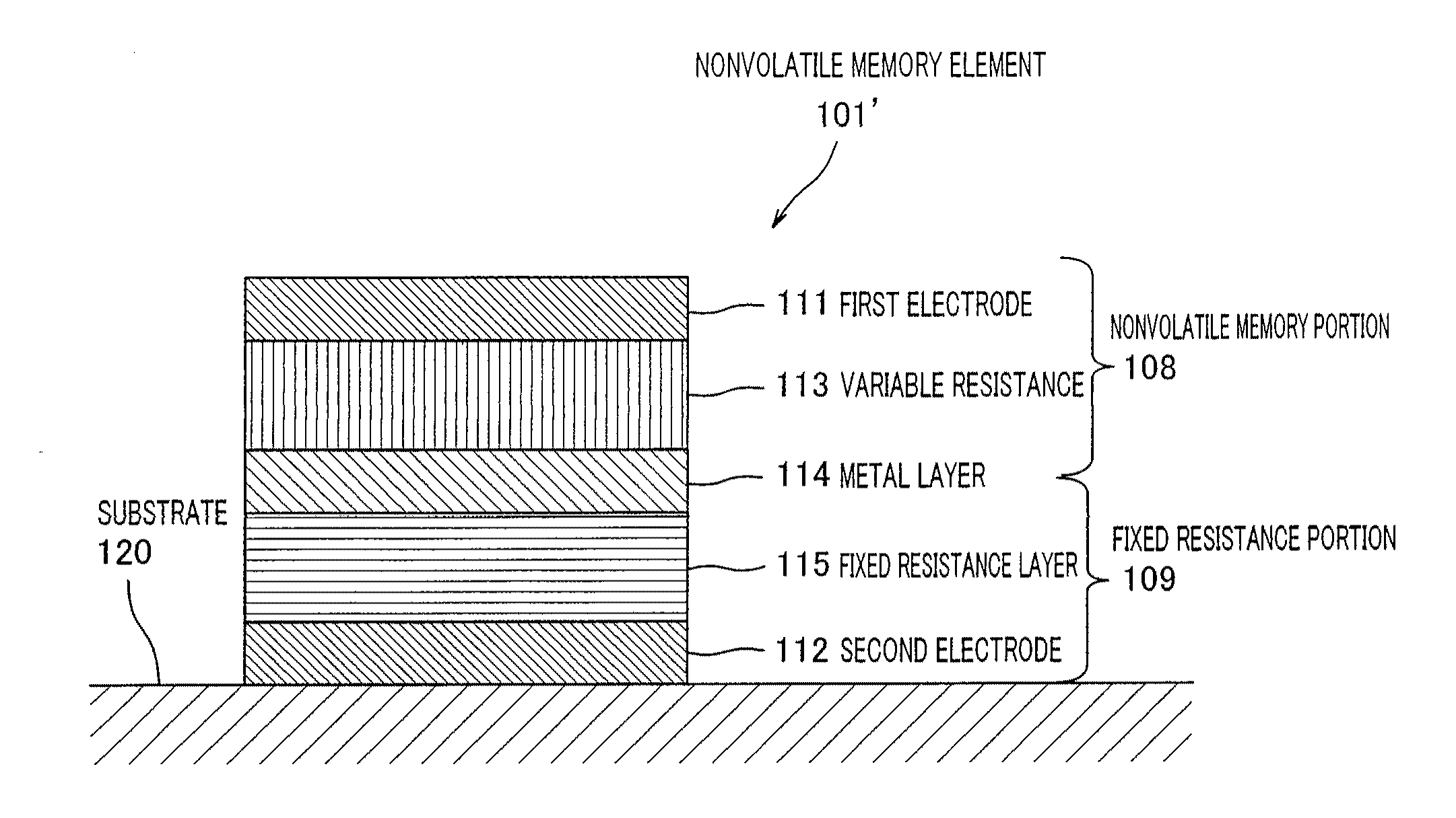
[0216]In Example, the nonvolatile memory apparatus shown in FIGS. 3 and 4 was manufactured, and electric pulses were applied to the nonvolatile memory apparatus. In this state, its operations was confirmed. Pt was used for the first electrode, the second electrode, and the metal layer. The thickness of the first electrode, the thickness of the second electrode, and the thickness of the metal layer were each set to 200 nm. The size of the first electrode, the size of the second electrode, and the size of the metal layer were each set to 3 μm2. The thickness of the variable resistance layer was set to 20 nm. The condition for forming the variable resistance layer was shown in table 1 as in Comparative example. In Example, when the tantalum oxide contained in the variable resistance layer is represented by TaOx, X was 1.2. As a material of the fixed resistance layer, Ni—Fe—O was used. The resistance value of the fixed resistance layer was controlled to be about 1000Ω.

[0217]In Example, ...

embodiment 2

[0224]A nonvolatile memory apparatus according to Embodiment 2 is a nonvolatile memory apparatus which includes the nonvolatile memory element according to Embodiment 1 and is a cross-point type memory apparatus in which an active layer intervenes at an intersection (three-dimensional cross point) between a word line and a bit line.

[0225][Configuration of Semiconductor Apparatus According to Embodiment 2]

[0226]FIG. 22 is a block diagram showing a configuration of a nonvolatile memory apparatus according to Embodiment 2 of the present invention. As shown in FIG. 22, a nonvolatile memory apparatus 200 according to this embodiment includes a memory main body 201 on a semiconductor substrate. The memory main body 201 includes a nonvolatile memory element array 202 (memory cell array), a row selection circuit / driver 203, a column selection circuit / driver 204, a write circuit 205 for writing data, a sense amplifier 206 which detects an amount of a current flowing in a selected bit line an...


PUM


Abstract

A nonvolatile memory apparatus comprises a first electrode (111), a second electrode (112), a variable resistance layer (113) which is disposed between the electrodes, a resistance value of the variable resistance layer reversibly varying between a plurality of resistance states based on an electric signal applied between the electrodes, a first terminal (103) connected to the first electrode, and a second terminal (104) connected to the second terminal. The variable resistance layer comprises at least a tantalum oxide, and is configured to satisfy 0<x<2.5 when the tantalum oxide is represented by TaOx; and wherein when a resistance value between the electrodes in a state where the variable resistance layer is in the low-resistance state is RL, a resistance value between the electrodes in a state where the variable resistance layer is in the high-resistance state is RH, and a resistance value of a portion other than the variable resistance layer in a current path connecting the first terminal to the second terminal via the first electrode, the variable resistance layer and the second electrode, is R0, R0 satisfies RL<R0.

Description

TECHNICAL FIELD[0001]The present invention relates to a nonvolatile memory apparatus, a nonvolatile memory element, and a nonvolatile memory element array. More particularly, the present invention relates to a resistance variable nonvolatile memory apparatus, a resistance variable nonvolatile memory element, and a resistance variable nonvolatile memory element array, whose resistance values vary according to electric signals applied.BACKGROUND ART[0002]With recent advancement of digital technologies, higher functionality of electronic hardware such as portable information devices and home information appliances have been brought out. For this reason, demands for an increase in a capacity of a nonvolatile memory element, a reduction in writing electric power, a reduction in write / read-out time, and longer life have been increasing.[0003]In response to such demands, it is said that there is a limitation on miniaturization of an existing flash memory using a floating gate. On the other...

Claims


Application Information

Patent Timeline
IPC IPC(8): H01L47/00H01L29/12
CPCG11C13/0007G11C13/003G11C2213/32G11C2213/74G11C2213/76G11C2213/79Y10S257/924H01L45/04H01L45/1233H01L45/146H01L45/1625H01L27/2409Y10S257/904H01L27/101H10B63/20H10N70/20H10N70/026H10N70/8833H10N70/826
Inventor OSANO, KOICHIFUJII, SATORUMURAOKA, SHUNSAKU
Owner PANASONIC SEMICON SOLUTIONS CO LTD
Learn More