
Drive circuit, light emitting diode head, and image forming apparatus

Active Publication Date: 2009-10-01
OKI DATA CORP
View PDF6 Cites 20 Cited by
  • Summary
  • Abstract
  • Description
  • Claims
  • Application Information

AI Technical Summary

Benefits of technology

[0030]In order to attain the objects described above, according to a first aspect of the present invention, a drive circuit includes a drive element for supplying a drive current to a driven element; a control voltage generation circuit for outputting a control voltage t

Problems solved by technology

As a result, the charged potential is discharged through the second MOS transistor and the LED without any control, thereby causing a sharp peak in a current waveform of the LED.
The peak thus created has a current value depending on a small wiring resistivity inside the drive circuit, and the current value is significant enough to deteriorate the LED, thereby reducing a lifetime thereof.
When such an excessive current flows in the LED element, even though it is for a short period of time, a large influence affects on the LED element, thereby deteriorating the LED element and changing a luminous efficiency thereof in a long run.
As described above, the overshoot of the drive current is regulated with the resistor element such as the on resistivity of the PMOS transistor 86, the wiring resistivity inside the LED element, and the likes, and it is difficult to accurately control the resistor element.
Accordingly, when an LED head includes a plurality of LED elements, each of the LED elements may have a different degree of deterioration after a long period of time, thereby causing a difference in a luminous efficiency thereof and causing an uneven print density.
Further, the conventional drive circuit has a noise voltage problem.
When the drive current flowing in a large number of the LED elements is turned off concurrently in a short period of time, a large noise voltage tends to be generated.
When all of the LED elements are turned on, the drive current becomes 5 A, so that the change in the drive current ΔI becomes 5 A. When such a large current is switched in a short period of time, a large noise voltage is generated, thereby causing malfunction of the drive circuit or even damaging the drive circuit.

Method used


Image

  • Drive circuit, light emitting diode head, and image forming apparatus
  • Drive circuit, light emitting diode head, and image forming apparatus
  • Drive circuit, light emitting diode head, and image forming apparatus

Examples


first embodiment

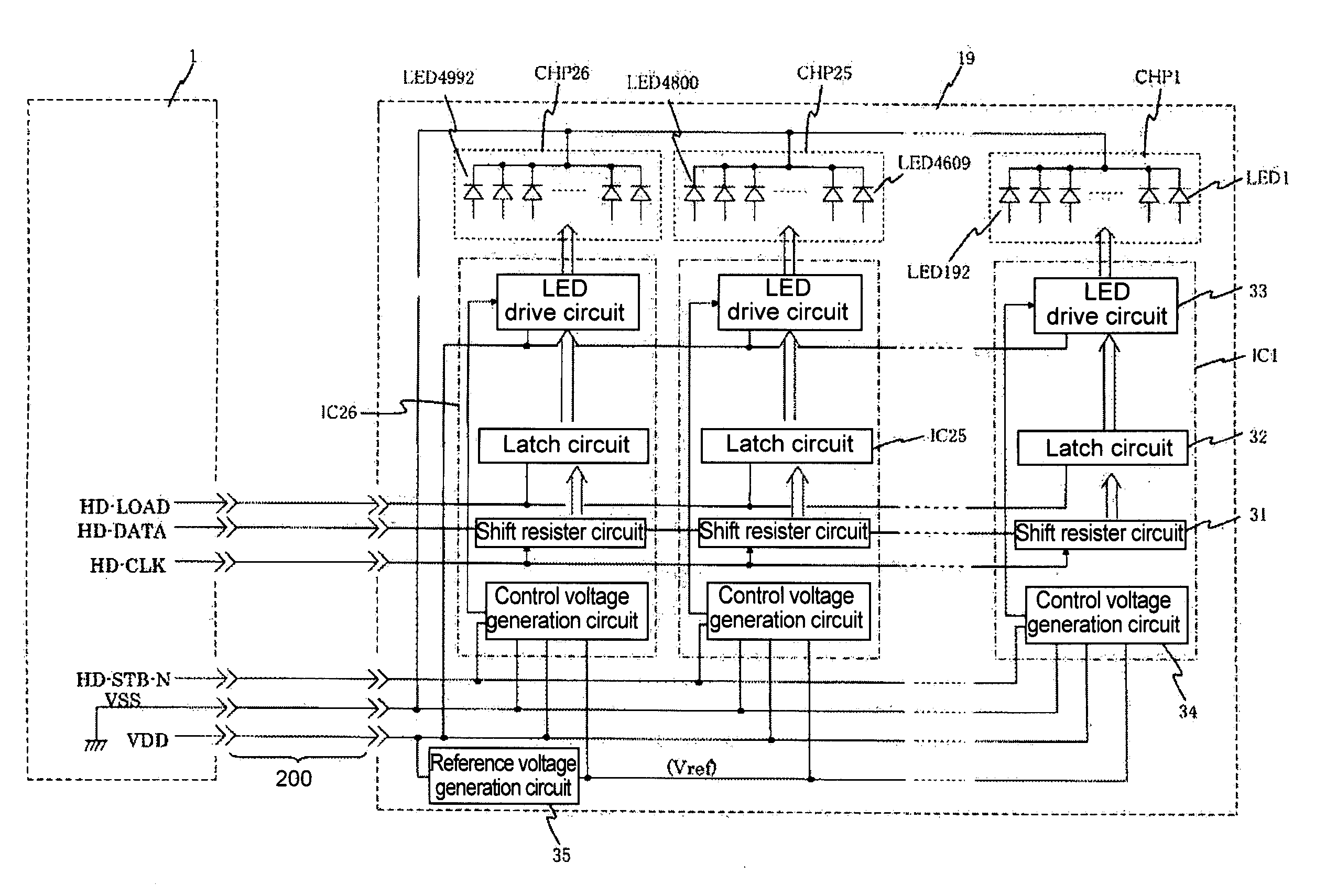
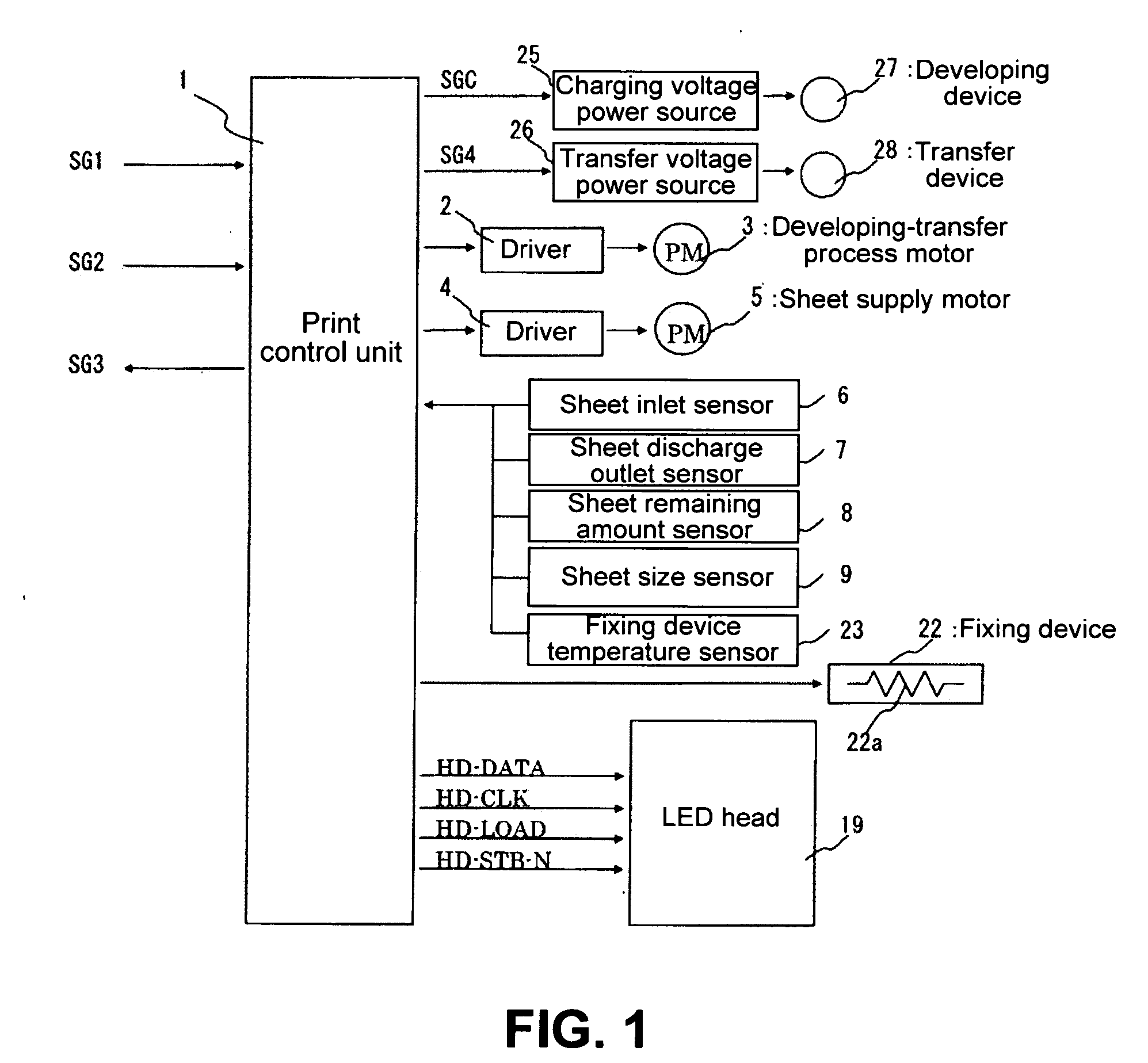
[0055]A first embodiment of the present invention will be explained. FIG. 1 is a block diagram showing a configuration of an electro-photography printer according to the first embodiment of the present invention.

[0056]In the embodiment, the electro-photography printer will be explained as an image forming apparatus. In the electro-photography printer, a charged photosensitive drum is selectively irradiated according to print information to form a static latent image. Then, toner is attached to the static latent image to form a toner image, and the toner image is transferred and fixed to a sheet.

[0057]As shown in FIG. 1, the electro-photography printer includes a print control unit 1 formed of a microprocessor, an RAM, an ROM, an input-output port, a timer, and the likes. The print control unit 1 is disposed in a printing unit of the electro-photography printer for performing a sequence control of an entire portion of the electro-photography printer and a printing operation according...

second embodiment

[0110]A second embodiment of the present invention will be explained next. FIG. 10 is a circuit diagram showing an LED drive main portion of a driver IC 123 according to the second embodiment of the present invention. A connection relationship between the LED drive circuit and a peripheral circuit thereof is shown in FIG. 10. In FIG. 10, the dot 1 (for example, a surrounding area of the drive circuit of the LED 1) is shown as an example.

[0111]In the second embodiment, the driver IC 123 includes a control voltage generation circuit 124 having a configuration different from that of the control voltage generation circuit 34 shown in FIG. 3 in the first embodiment. Other similar elements are designated with the same reference numerals.

[0112]As shown in FIG. 10, the driver IC 123 includes the control voltage generation circuit 124. The control voltage generation circuit 124 includes an operational amplifier 122 having an output potential Vcon. The resistor 63 has the resistivity of Rref....

third embodiment

[0133]A third embodiment of the present invention will be explained next. FIG. 14 is a circuit diagram showing an LED drive main portion of a driver IC 126 according to the third embodiment of the present invention. A connection relationship between the LED drive circuit and a peripheral circuit thereof is shown in FIG. 14. In FIG. 14, the dot 1 (for example, a surrounding area of the drive circuit of the LED 1) is shown as an example.

[0134]In the third embodiment, the driver IC 126 includes a control voltage generation circuit 127 having a configuration different from that of the control voltage generation circuit 34 shown in FIG. 3 in the first embodiment. Other similar elements are designated with the same reference numerals.

[0135]As shown in FIG. 14, the driver IC 126 includes the control voltage generation circuit 127. The control voltage generation circuit 127 includes the operational amplifier 61 having the output potential Vcon. The resistor 63 has the resistivity of Rref. T...


PUM


Abstract

A drive circuit includes a drive element for supplying a drive current to a driven element; a control voltage generation circuit for outputting a control voltage to the drive element to generate the drive current through inputting a reference voltage; and a switch section for shutting down the reference voltage when the driven element is not driven so that the control voltage decreases to a level not to generate the drive current.

Description

BACKGROUND OF THE INVENTION AND RELATED ART STATEMENT[0001]The present invention relates to a drive circuit for driving a group of driven elements such as, for example, an array of light emitting diodes (LEDs) disposed in an electro-photography printer as a light source, an array of heating resistors disposed in a thermal printer, and an array of display units disposed in a display device. The present invention also relates to a light emitting diode (LED) head including the drive circuit; and an image forming apparatus including the light emitting diode (LED) head.[0002]In the specification, a light emitting diode may be referred to as an LED; a monolithic integrated circuit may be referred to as an IC; an n-channel MOS (Metal Oxide Semiconductor) transistor may be referred to as an NMOS transistor; and a p-channel MOS transistor may be referred to as a PMOS transistor.[0003]Further, a high signal level may be referred to as a logical value of one (1), and a low signal level may be ...

Claims


Application Information

Patent Timeline
IPC IPC(8): H05B41/36H03K3/00B41J2/44G03G15/04B41J2/45B41J2/455H01L33/00H01L33/08H01L33/30H01L33/58H01L33/62H04N1/036
CPCG03G15/326G06K15/1247H01L2924/1301H01L2924/13091H01L2924/30107B41J2/45H01L2924/3011H01L2224/48091G03G15/043G03G15/04054G09G2330/028G09G3/32G09G2310/0286G09G2310/0294H01L2924/00014H01L2924/00
Inventor NAGUMO, AKIRA
Owner OKI DATA CORP
Learn More