
Integrated Circuit Chip Design Flow Methodology Including Insertion of On-Chip or Scribe Line Wireless Process Monitoring and Feedback Circuitry

a technology of integrated circuits and process monitoring, applied in semiconductor/solid-state device testing/measurement, total factory control, instruments, etc., can solve problems such as the inability to control processes to tighter tolerances, the inability to create trade-offs between timing margin, power and performance, and the inability to achieve the effect of tight tolerances

Active Publication Date: 2009-09-24
MARVELL ASIA PTE LTD
View PDF9 Cites 20 Cited by
  • Summary
  • Abstract
  • Description
  • Claims
  • Application Information

AI Technical Summary

Benefits of technology

The patent describes a system and method for designing and manufacturing integrated circuit chips. The system includes a library of pre-qualified intra-process monitoring circuits and a design data analyzer that identifies the components of the chip design. The intra-process monitoring circuits are selected from the library and the design data is modified to include the monitoring circuits. The design data is then sent to a design data editor for further modification. The method also includes generating an extension to a test program for monitoring parameters of the chip components during wafer fabrication and initiating wafer manufacturing. The system and method allow for wireless intra-process monitoring of chip components during manufacturing and adjustment of manufacturing process steps based on the results of the monitoring.

Problems solved by technology

As lithographic geometries are reduced for each successive semiconductor process generation, the effects of process variability have become significant first order issues.
Designers are faced with creating tradeoffs between timing margin, power, and performance.
The ability to control processes to tighter tolerances is limited by an inability to obtain actual inline (i.e., intra-process) integrated circuit parameter measurements for a given wafer or die or for a given site on a given wafer or die.
Unfortunately, the limited frequency and number of sites sampled limits the tightness of control through such historical methods.

Method used


Image

  • Integrated Circuit Chip Design Flow Methodology Including Insertion of On-Chip or Scribe Line Wireless Process Monitoring and Feedback Circuitry
  • Integrated Circuit Chip Design Flow Methodology Including Insertion of On-Chip or Scribe Line Wireless Process Monitoring and Feedback Circuitry
  • Integrated Circuit Chip Design Flow Methodology Including Insertion of On-Chip or Scribe Line Wireless Process Monitoring and Feedback Circuitry

Examples


Embodiment Construction

[0029]The embodiments of the invention and the various features and advantageous details thereof are explained more fully with reference to the non-limiting embodiments that are illustrated in the accompanying drawings and detailed in the following description.

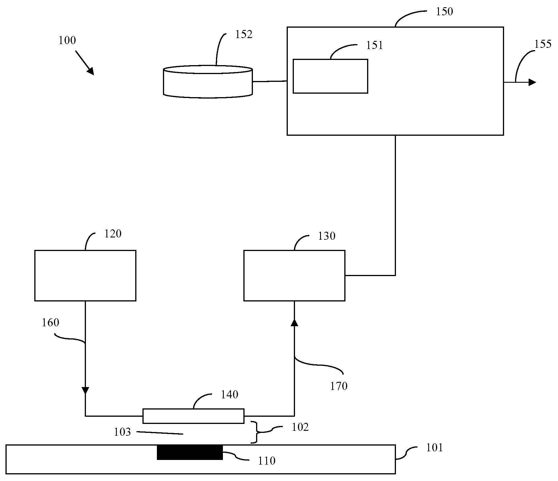
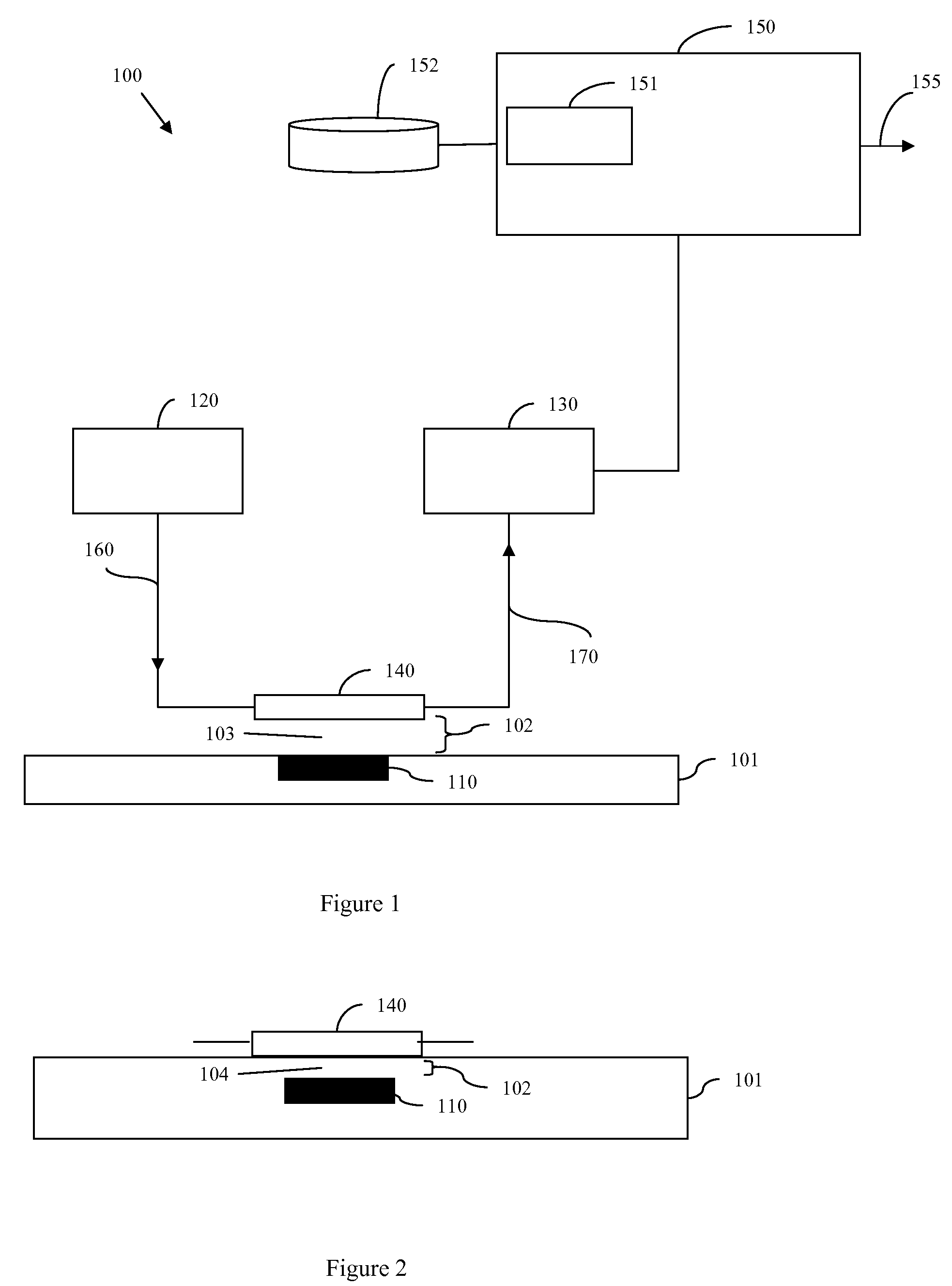
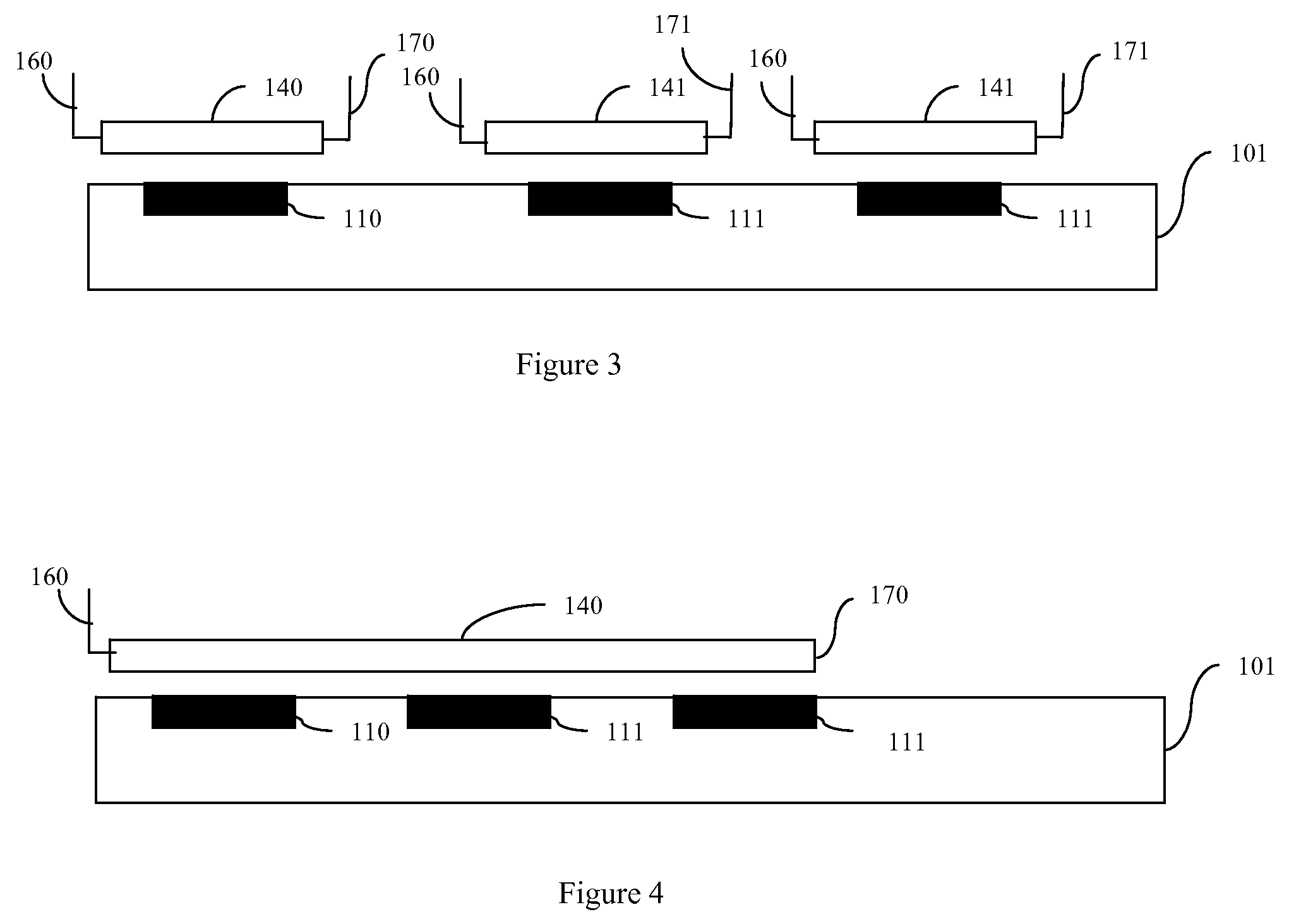
[0030]As mentioned above, as lithographic geometries are reduced for each successive semiconductor process generation, the effects of process variability have become significant first order issues. Designers are faced with creating tradeoffs between timing margin, power, and performance. Tighter process controls would enable lower power, higher performance, and / or higher yielding products. The ability to control processes to tighter tolerances is limited by an inability to obtain actual inline (i.e., intra-process) integrated circuit parameter measurements for a given wafer or die or for a given site on a given wafer or die

[0031]Current techniques for taking integrated circuit parameter measurements utilize wired mechanical pr...


PUM


Abstract

Disclosed are embodiments of a design and manufacturing system and an associated method that allow for design analysis and for insertion, during wafer manufacture, of intra-process monitoring circuitry. These embodiments use a library of pre-qualified intra-process monitoring circuits and a cross-correlation table that links different monitoring circuits with different IC chip components. Specifically, these embodiments analyze integrated circuit chip design data to identify the components designed into the chip. Then, one or more intra-process monitoring circuits are selected from the library and the design data is modified to include the selected monitoring circuit(s).

Description

CROSS-REFERENCE TO RELATED APPLICATIONS [0001]The present invention claims the benefit under 35 U.S.C. §120 as a continuation-in-part of presently pending U.S. patent application Ser. No. 12 / 053,705 entitled “SYSTEM AND METHOD FOR WIRELESS AND DYNAMIC INTRA-PROCESS MEASUREMENT OF INTEGRATED CIRCUIT PARAMETERS”, filed on Mar. 24, 2008 with multiple common inventors, the entire teachings of which are incorporated herein by reference.BACKGROUND [0002]1. Field of the Invention[0003]The embodiments of the invention generally relate to intra-process monitoring circuits and, more particularly, to an integrated circuit (IC) chip design and manufacturing system and an associated design and manufacturing flow method that provide for chip design analysis and insertion of on-chip and / or within scribe line intra-process monitoring circuits.[0004]2. Description of the Related Art[0005]As lithographic geometries are reduced for each successive semiconductor process generation, the effects of proce...

Claims


Application Information

Patent Timeline
Patent Type & Authority Applications(United States)
IPC IPC(8): G06F17/50H01L21/66
CPCG01R31/2884G01R31/3025G06F17/5045G06F2217/12H01L2924/0002H01L2924/00G06F30/30G06F2119/18Y02P90/02
Inventor ANEMIKOS, THEODOROSHALL, EZRA D.B.VENTRONE, SEBASTIAN T.
Owner MARVELL ASIA PTE LTD
Learn More