Vertical light emitting diode and method of manufacturing the same

a technology of light-emitting diodes and vertical layers, which is applied in the direction of semiconductor/solid-state device manufacturing, electrical equipment, semiconductor devices, etc., can solve the problems of poor thermal conductivity, rigid non-conducting substrates, and limitation in reducing manufacturing costs, so as to increase the surface electron concentration of n-type gan layers and enhance thermal stability

Active Publication Date: 2009-09-03
SAMSUNG ELECTRONICS CO LTD
View PDF8 Cites 206 Cited by
  • Summary
  • Abstract
  • Description
  • Claims
  • Application Information

AI Technical Summary

Benefits of technology

[0013]An advantage of the present invention is that it provides a vertical LED in which the surface of an n-type GaN layer coming in contact with an n-electrode is formed of a Ga+N layer containing a larger amount of Ga than that of N, that is, the surface electron concentration of the n-type GaN layer is increased. In the vertical LED, the contact resistance of the n-type GaN layer coming in contact with the n-electrode and having an N-face or N-polar surface can be reduced, and thermal stability can be enhanced.
[0014]Another advantage of the invention is that is provides a method of manufacturing the vertical LED.
[0015]Additional aspect and advantages of the present general inventive concept will be set forth in part in the description which follows and, in part, will be obvious from the description, or may be learned by practice of the general inventive concept.
[0016]According to an aspect of the invention, a vertical LED comprises an n-electrode; an n-type GaN layer formed under the n-electrode, the n-type GaN layer having a surface coming in contact with the n-electrode, the surface having a Ga+N layer containing a larger amount of Ga than that of N; an active layer formed under the n-type GaN layer; a p-type GaN layer formed under the active layer; a p-electrode formed under the p-type GaN layer; and a structure support layer formed under the p-electrode.
[0017]The n-electrode may be formed of a single layer composed of one or more metals selected from the group consisting of Ti, Ta, and Zr. Alternately, the n-electrode may be formed of a multilayer in which more than two layers including a layer composed of one or more metals selected from the group consisting of Ti, Ta, and Zr are laminated.
[0018]The Ga+N layer of the n-type GaN layer may be formed by laser-treating or heat-treating the surface of the n-type GaN layer coming in contact with the n-electrode.

Problems solved by technology

Generally, a nitride-based semiconductor LED is grown on a sapphire substrate, but the sapphire substrate is a rigid nonconductor and has poor thermal conductivity.
Therefore, there is a limitation in reducing the manufacturing costs by reducing the size of a nitride-based semiconductor LED, or improving the optical power and chip characteristic.

Method used


Image

  • Vertical light emitting diode and method of manufacturing the same
  • Vertical light emitting diode and method of manufacturing the same
  • Vertical light emitting diode and method of manufacturing the same

Examples


Embodiment Construction

[0030]Reference will now be made in detail to the embodiments of the present general inventive concept, examples of which are illustrated in the accompanying drawings, wherein like reference numerals refer to like elements throughout. The embodiments are described below in order to explain the present general inventive concept by referring to the figures. In the drawings, the thicknesses of layers and regions are exaggerated for clarity.

[0031]Hereinafter, preferred embodiments of the present invention will be described in detail with reference to the accompanying drawings.

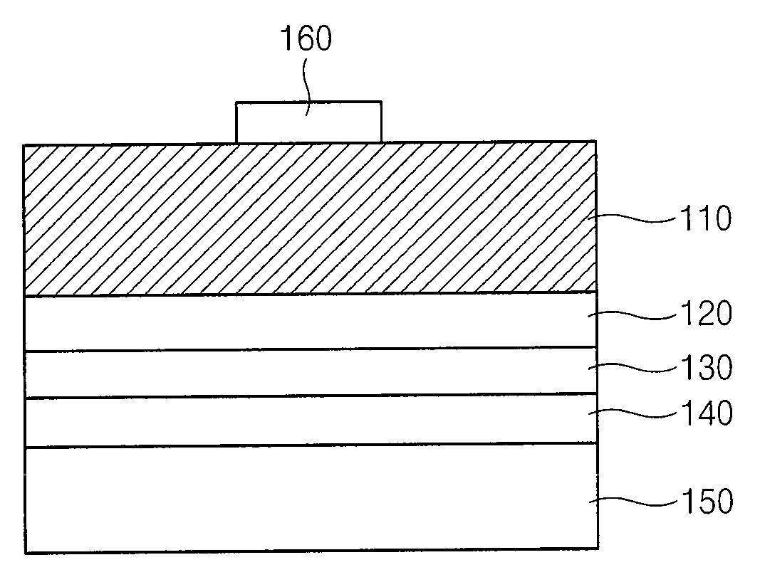
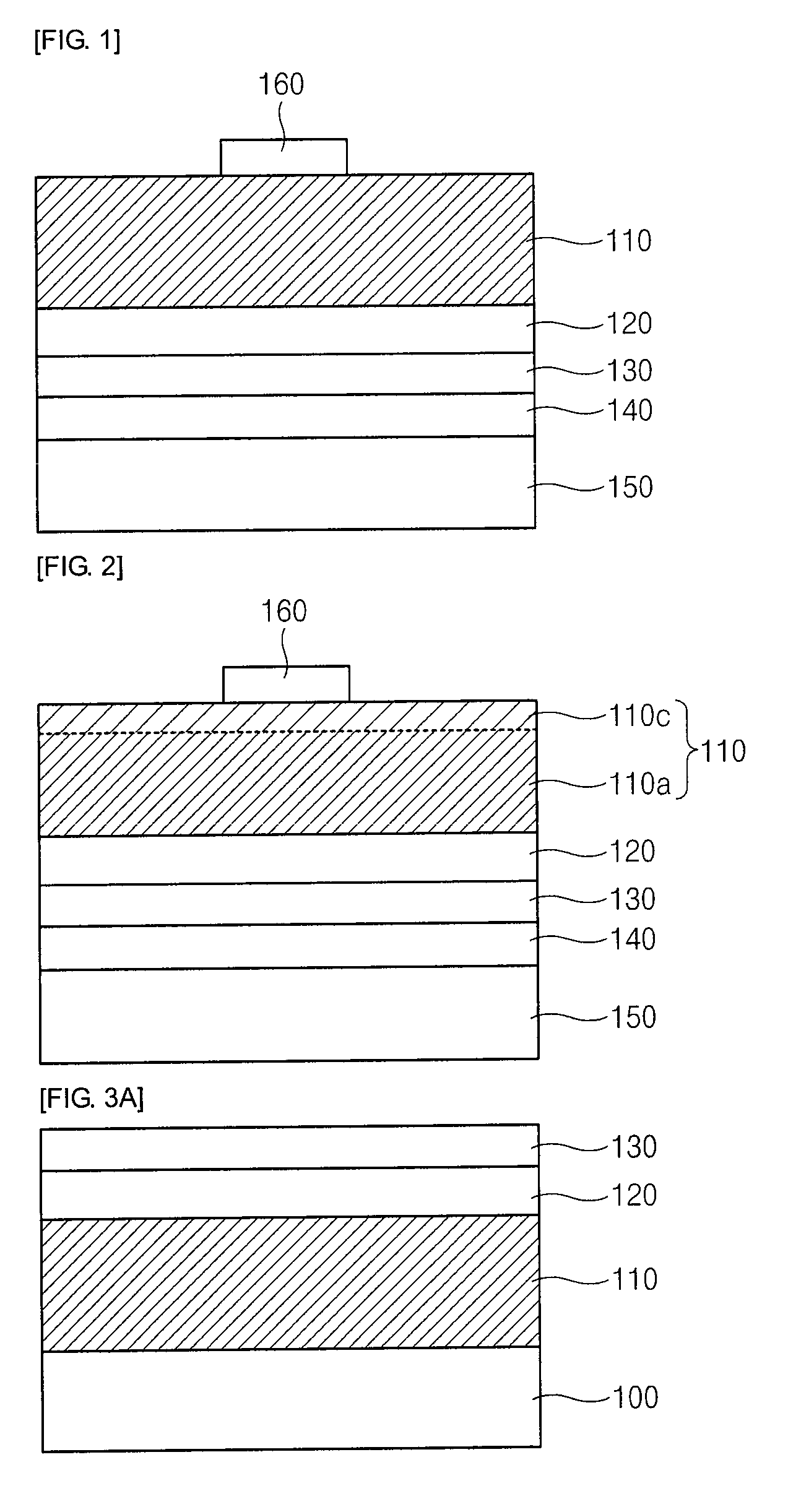
[0032]Structure of Vertical LED

[0033]Referring to FIG. 2, the structure of a vertical LED according to an embodiment of the invention will be described in detail.

[0034]FIG. 2 is a cross-sectional view of a vertical LED according to an embodiment of the invention.

[0035]As shown in FIG. 2, the vertical LED has an n-electrode 160 formed in the uppermost portion thereof. Preferably, the n-electrode 160 is formed of a s...


PUM


Abstract

Provided is a vertical LED including an n-electrode; an n-type GaN layer formed under the n-electrode, the n-type GaN layer having a surface coming in contact with the n-electrode, the surface having a Ga+N layer containing a larger amount of Ga than that of N; an active layer formed under the n-type GaN layer; a p-type GaN layer formed under the active layer; a p-electrode formed under the p-type GaN layer; and a structure support layer formed under the p-electrode.

Description

CROSS-REFERENCE TO RELATED APPLICATIONS[0001]This application claims the benefit of Korean Patent Application No. 10-2006-0102967 filed with the Korean Intellectual Property Office on Oct. 23, 2006, the disclosure of which is incorporated herein by reference.BACKGROUND OF THE INVENTION[0002]1. Field of the Invention[0003]The present invention relates to a vertical light emitting diode (LED) and a method of manufacturing the same, which can reduce contact resistance of an negative electrode formed on the surface of an n-type GaN layer and can enhance thermal stability.[0004]2. Description of the Related Art[0005]Generally, a nitride-based semiconductor LED is grown on a sapphire substrate, but the sapphire substrate is a rigid nonconductor and has poor thermal conductivity. Therefore, there is a limitation in reducing the manufacturing costs by reducing the size of a nitride-based semiconductor LED, or improving the optical power and chip characteristic. Particularly, because the app...

Claims


Application Information

Patent Timeline
Patent Type & Authority Applications(United States)
IPC IPC(8): H01L21/28H01L33/32
CPCH01L33/32H01L33/14H01L33/40
Inventor LEE, SU YEOLYOON, SANG HOBAIK, DOO GOCHOI, SEOK BEOMJANG, TAE SUNGWOO, JONG GUN
Owner SAMSUNG ELECTRONICS CO LTD
Why Eureka
Try Eureka