
Memory controller, memory system, and access control method of flash memory

a memory controller and access control technology, applied in the direction of memory adressing/allocation/relocation, instruments, fault response, etc., can solve the problem that the data in the nand flash memory cannot be read properly, the rate of accessing outside of an application specific integrated circuit (asic) chip is increased, and it is impossible for another master to access the ram

Inactive Publication Date: 2009-08-27
KK TOSHIBA
View PDF6 Cites 67 Cited by
  • Summary
  • Abstract
  • Description
  • Claims
  • Application Information

AI Technical Summary

Problems solved by technology

At the time of writing write data into the NAND flash memory, because the write data is written after adding the ECC in the write data, when the write data is written in a situation where the data size of the write data is less than the page size of the NAND flash memory, there are cases that the data in the NAND flash memory cannot be read properly due to generation of an ECC error at the time of subsequent data reading.
However, when the dummy data is prepared on a RAM on the side of the FW, there is a rise in the usage of the RAM capacity for saving the dummy data and also a rise in the usage rate of a bus by an amount of dummy data when writing the write data into the NAND flash memory from the RAM, which makes it impossible for another master to access the RAM.
There is another problem such that when the write data and the dummy data are prepared in a DRAM outside of a chip having a memory controller, the rate of accessing outside of an application specific integrated circuit (ASIC) chip is increased, which results in higher power consumption.

Method used


Image

  • Memory controller, memory system, and access control method of flash memory
  • Memory controller, memory system, and access control method of flash memory
  • Memory controller, memory system, and access control method of flash memory

Examples


embodiments

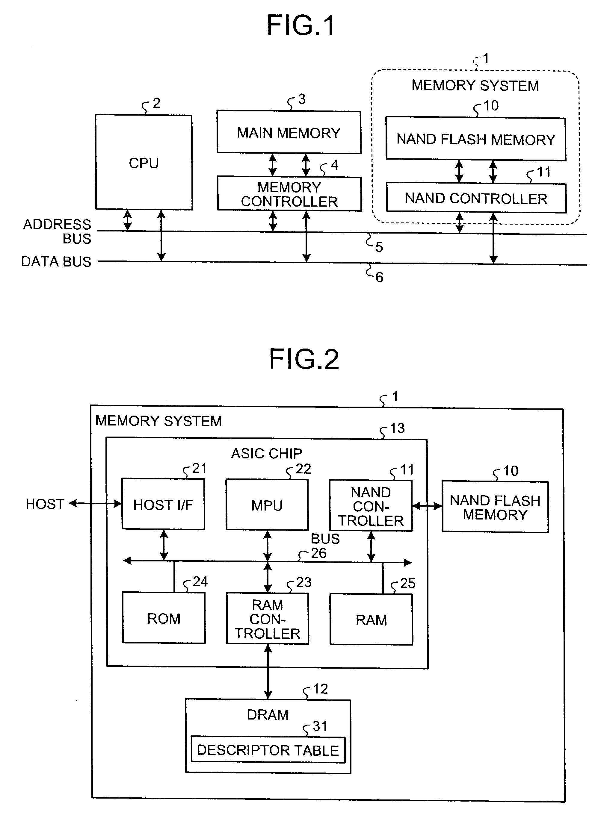
[0022]FIG. 1 is a schematic diagram of an example of a computing system including a memory system 1 according to an embodiment of the present invention. The memory system 1 is a memory device connected to a not shown host device (such as a personal computer (PC)).

[0023]The computing system includes a CPU 2, a main memory 3 such as a DRAM, a memory controller 4 that controls the main memory 3, and the memory system 1. The CPU 2, the main memory 3, and the memory system 1 are connected to each other via an address bus 5 that handles addresses and a data bus 6 that handles data.

[0024]In this computing system, in response to a transfer request (a read request or a write request) from the CPU 2, data in the CPU 2 (including data input from outside) or data in the main memory 3 is transferred to the memory system 1 when the transfer request is a write request, and data in the memory system 1 is transferred to either the CPU 2 or the main memory 3 when the transfer request is a read reques...


PUM


Abstract

A memory controller adds dummy data to write data by referring to instruction information about a descriptor transfer of the write data if a size of the write data to be written according to a data-write request information does not match a page size unit, thereby adjusting the size of the write data to the page size unit and then outputs the write data.

Description

CROSS-REFERENCE TO RELATED APPLICATIONS[0001]This application is based upon and claims the benefit of priority from the prior Japanese Patent Application No. 2008-046705, filed on Feb. 27, 2008; the entire contents of which are incorporated herein by reference.BACKGROUND OF THE INVENTION[0002]1. Field of the Invention[0003]The present invention relates to a memory controller, a memory system, and an access control method of a flash memory.[0004]2. Description of the Related Art[0005]Recently, non-volatile semiconductor memories are used in various devices ranging from large-scale computers to personal computers, home appliances, cellular phones or the like. A NAND flash memory in particular is a non-volatile, large capacity, and highly integrated semiconductor memory in which data can be rewritten electrically, and it is considered as an alternative to hard disk drives (HDDs).[0006]JP-A 2007-87388 (KOKAI) discloses a data processing system that employs a NAND flash memory. In this d...

Claims


Application Information

Patent Timeline
Patent Type & Authority Applications(United States)
IPC IPC(8): G06F12/02G06F12/00
CPCG06F12/0246Y02B60/1225G06F2212/7203Y02D10/00
Inventor YASUFUKU, KENTA
Owner KK TOSHIBA
Learn More