Semiconductor device and manufacturing method and mounting method thereof
a semiconductor device and manufacturing method technology, applied in semiconductor devices, semiconductor/solid-state device details, electrical devices, etc., can solve the problems of increasing manufacturing cost and manufacturing time, and achieve the effect of reducing the mounting height of the semiconductor device mounted on the mounting substrate, preventing degradation of parallelism, and easy improvement of parallelism
- Summary
- Abstract
- Description
- Claims
- Application Information
AI Technical Summary
Benefits of technology
Problems solved by technology
Method used
Image

Examples
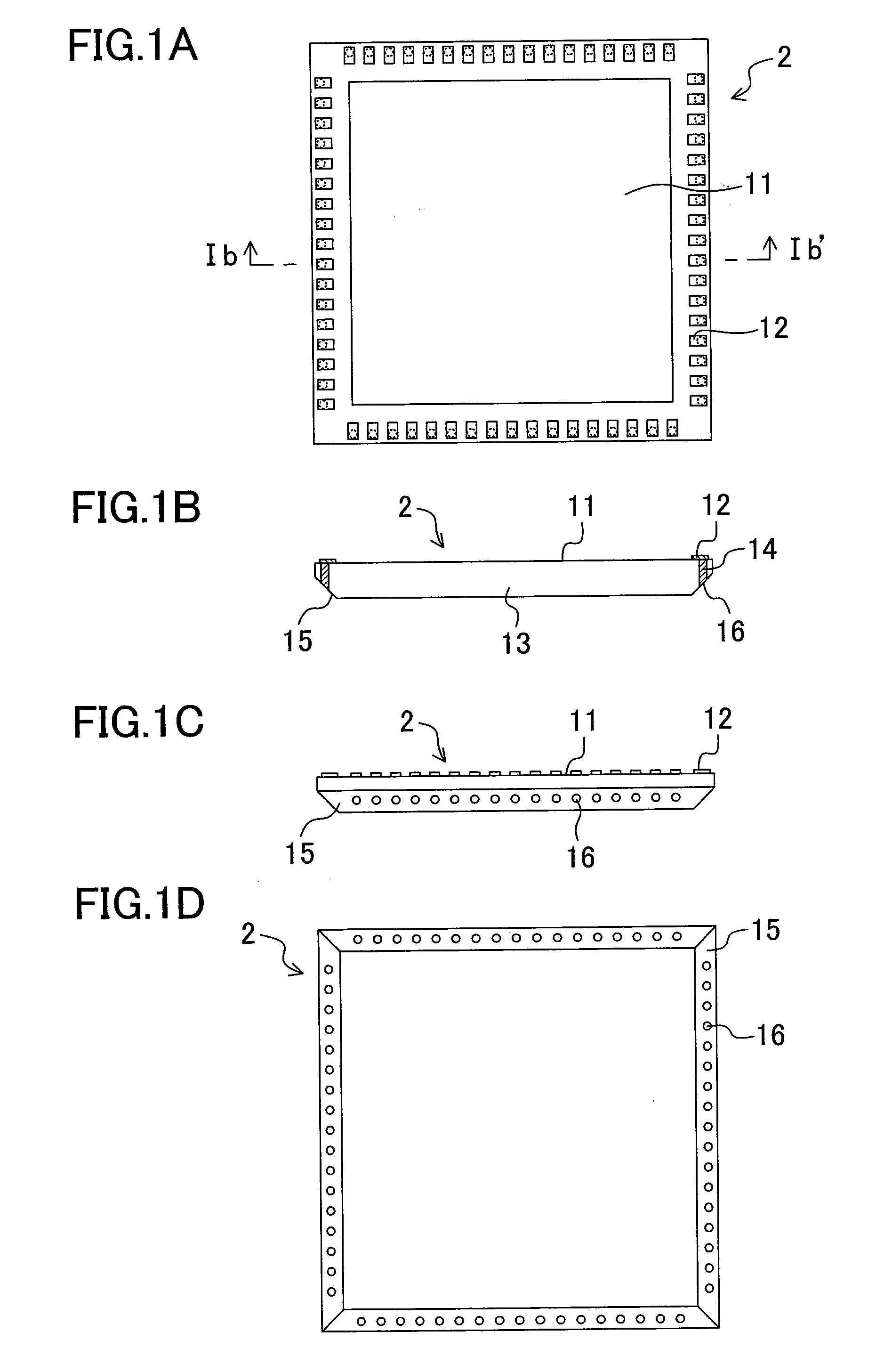
first embodiment
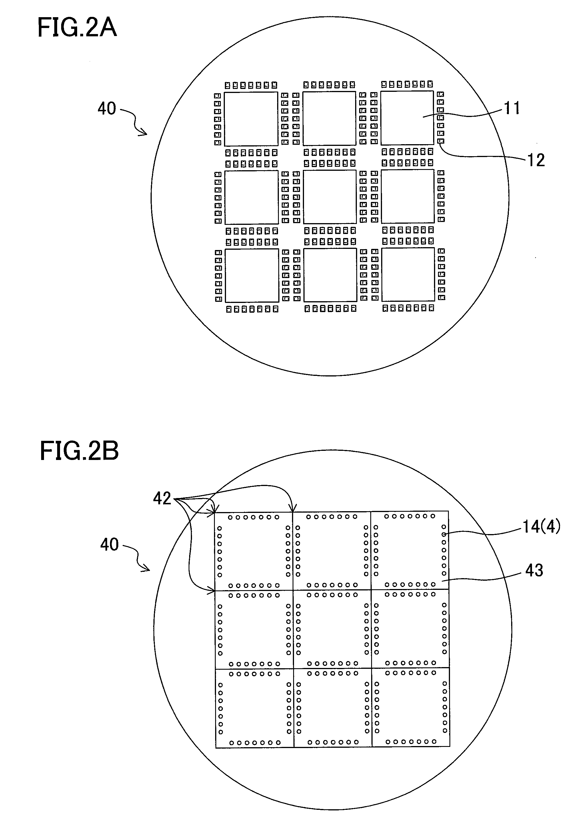
[0057]FIGS. 1A through 1D are diagrams showing a semiconductor device 2 according to a first embodiment. FIG. 1A is a plan view showing the semiconductor device 2 viewed from the front surface thereof, FIG. 1B is a cross-sectional view taken along line Ib-Ib′ in FIG. 1A, FIG. 1C is a side view, and FIG. 1D is a bottom view of the semiconductor device 2 viewed from the back surface thereof. As described above, in this embodiment, a solid-state imaging device is described as an example of the semiconductor device 2.
[0058]As shown in FIGS. 1A through 1D, the semiconductor device 2 of this embodiment is formed by using a semiconductor substrate 13 made of silicon. The semiconductor device 2 has an active region 11 on a surface thereof and electrode pads 12 on a peripheral portion of the surface. (As shown particularly in FIG. 1B), through holes are formed in the semiconductor substrate 13 so as to extend from the back surface of the semiconductor substrate 13 to the electrode pads 12. T...
second embodiment
[0105]Hereinafter, a semiconductor device 2a and a mounting method thereof according to a second embodiment of the invention will be described with reference to the figures. FIG. 6A is a cross-sectional view of the semiconductor device 2a of the second embodiment mounted on a mounting substrate 30a, and FIG. 6B is an enlarged view of a region around a peripheral portion of the semiconductor device 2a in FIG. 6A.
[0106]As shown in FIGS. 6A and 6B, the semiconductor device 2a further includes bumps 32 on external electrodes 16 in addition to the structure of the semiconductor device 2 of the first embodiment. The bumps 32 are made of a conductive metal material such as solder bumps, Au bumps, Au stat bumps, and Cu bumps and protrude from the surface of the external electrodes 16. Other elements are denoted with the same reference numerals as those of the semiconductor device 2 and detailed description thereof will be omitted.
[0107]An electrode pattern 17 on a mounting substrate 30a has...
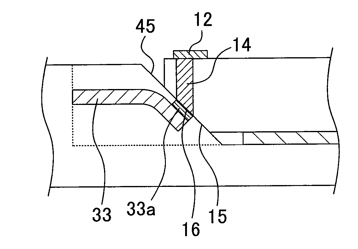
third embodiment
[0111]Hereinafter, a semiconductor device 2b and a mounting method thereof according to a third embodiment of the invention will be described with reference to the figures. FIG. 7A is a cross-sectional view of the semiconductor device 2b of the third embodiment mounted on a mounting substrate 30b, and FIG. 7B is an enlarged view of a region around a peripheral portion of the semiconductor device 2b in FIG. 7A.
[0112]Since the semiconductor device 2b is the same as the semiconductor device 2 of the first embodiment, detailed description thereof will be omitted.
[0113]As shown in FIGS. 7A and 7B, the mounting substrate 30b includes a tilted surface 45 that is in contact with a cutting surface 15 of the semiconductor device 2b, and an electrode pattern 33 that is electrically connected to external electrodes 16. The electrode pattern 33 is made of a material having a spring property (an elastic deformation region). The material may be a metal material such as Cu and spring steel, or a co...
PUM
 Abstract
Description
Claims
Application Information
 - R&D
- Intellectual Property
- Life Sciences
- Materials
- Tech Scout
- Unparalleled Data Quality
- Higher Quality Content
- 60% Fewer Hallucinations
Browse by: Latest US Patents, China's latest patents, Technical Efficacy Thesaurus, Application Domain, Technology Topic, Popular Technical Reports.
© 2025 PatSnap. All rights reserved.Legal|Privacy policy|Modern Slavery Act Transparency Statement|Sitemap|About US| Contact US: help@patsnap.com