All-silicon raman amplifiers and lasers based on micro ring resonators

a raman laser and amplifier technology, applied in the direction of lasers using scattering effects, laser details, electrical equipment, etc., can solve the problems of monolithic silicon chip microscopic low-threshold raman amplification and lasing devices that have yet to be developed

Inactive Publication Date: 2009-07-30
THE TRUSTEES OF COLUMBIA UNIV IN THE CITY OF NEW YORK
View PDF24 Cites 19 Cited by
  • Summary
  • Abstract
  • Description
  • Claims
  • Application Information

AI Technical Summary

Problems solved by technology

Despite these advances, microscopic low-threshold Raman amplification and lasing devices on a monolithic silicon chip has yet to be developed.

Method used


Image

  • All-silicon raman amplifiers and lasers based on micro ring resonators
  • All-silicon raman amplifiers and lasers based on micro ring resonators
  • All-silicon raman amplifiers and lasers based on micro ring resonators

Examples


Embodiment Construction

, including the description of various embodiments of the invention, will be best understood when read in reference to the accompanying figures wherein:

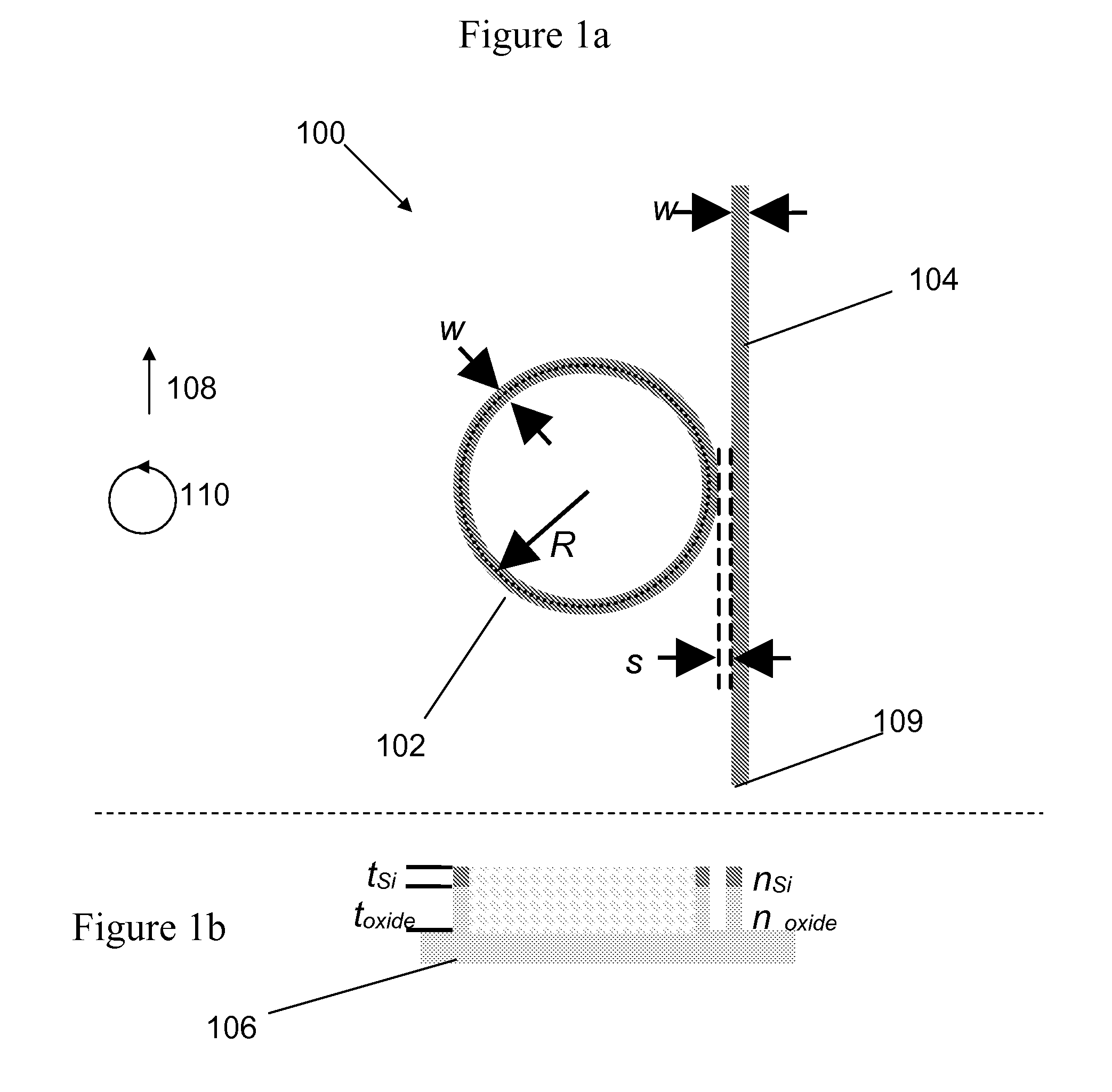
[0011]FIG. 1a is a top view of a Raman amplification and lasing device in accordance with various embodiments of the present invention;

[0012]FIG. 1b is a cross-sectional view of the Raman amplification and lasing device in FIG. 1a;

[0013]FIG. 2 is a transmission spectrum of a Raman amplification and lasing device according to one example of the present invention;

[0014]FIG. 3 is a diagram illustrating the WGMs formed by a beam of light in the same example device as used for FIG. 2;

[0015]FIG. 4 is a diagram illustrating the WGMs formed by another beam of light in the same example device as used for FIG. 2;

[0016]FIG. 5 is a flow chart illustrating methods for manufacturing a Raman amplification and lasing device according to various embodiments of the present invention; and

[0017]FIG. 6 is a top view of a fabricated Raman amplification a...


PUM


Abstract

Methods of manufacturing a lasing device are provided by some embodiments, the methods including: creating a silicon micro ring with a predetermined radius and a predetermined first cross-sectional dimension; creating a silicon waveguide with a predetermined second cross-sectional dimension, the silicon waveguide spaced from the silicon micro ring by a predetermined distance; and wherein the predetermined distance, the predetermined radius, the predetermined first cross-sectional dimension, and the predetermined second cross-sectional dimension are determined so that at least one first whispering gallery mode resonant frequency of the silicon micro ring and at least one second whispering gallery mode resonant frequency of the silicon micro ring are separated by an optical phonon frequency of silicon.

Description

RELATED APPLICATIONS[0001]This application is a divisional of U.S. patent application Ser. No. 11 / 354,725, filed Feb. 15, 2006, which claims the benefit under 35 U.S.C. §119(e) of U.S. Provisional Patent Application No. 60 / 653,556, filed on Feb. 16, 2005, each of which is hereby incorporated herein by reference in its entirety.FIELD OF THE INVENTION[0002]The present invention relates to optical amplification and lasing devices, and methods for manufacturing the devices. More particularly, the present invention relates to low-threshold microcavity Raman lasers, and methods for manufacturing the same.BACKGROUND OF THE INVENTION[0003]Stimulated Raman scattering (“SRS”) has a rich and evolving history since the development of the laser. In 1962, SRS effect at infrared frequencies was discovered. This discovery was soon described as a two-photon process with a full quantum mechanical calculation. To account for anti-Stokes generation and higher-order Raman effects, however, coupled-wave ...

Claims


Application Information

Patent Timeline
Patent Type & Authority Applications(United States)
IPC IPC(8): H01L21/00
CPCH01S3/0632H01S3/083H01S3/30H01S3/1628H01S3/2308H01S3/094096
Inventor YANG, XIAODONGWONG, CHEE WEI
Owner THE TRUSTEES OF COLUMBIA UNIV IN THE CITY OF NEW YORK
Why Eureka
Try Eureka