
Avoiding floating diffusion contamination

a technology of floating diffusion and contamination, applied in the direction of code conversion, pulse technique, instruments, etc., can solve the problem of undeterministic coupling amount of floating diffusion back onto the net, and achieve the effect of reducing the capacitance contribution of the net, reducing the influence of follow on the circuit, and reducing the effect of the capacitance contribution

Active Publication Date: 2009-07-16
INTERSIL INC
View PDF8 Cites 2 Cited by
  • Summary
  • Abstract
  • Description
  • Claims
  • Application Information

AI Technical Summary

Benefits of technology

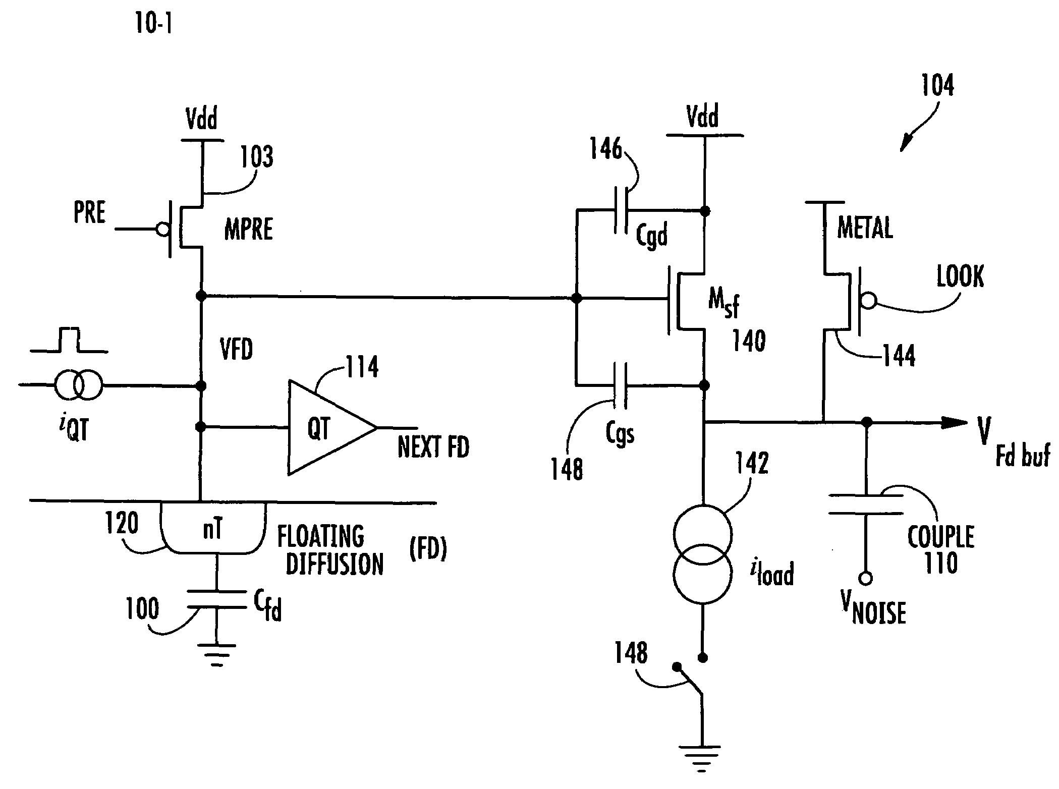
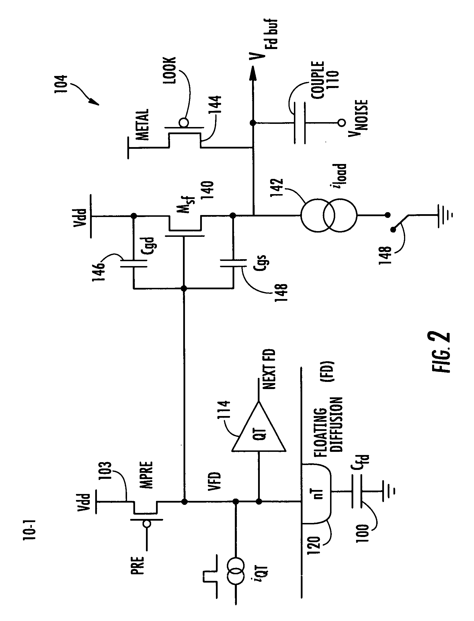
[0006]The known state in the SFB circuit may be imposed by using a Metal Oxide Semiconductor Field Effect Transistor (MOSFET) controlled by a clock signal. In one embodiment, the clock signal is arrange to hold the output of the SFB circuit in a known high state prior to charge transfer onto the floating diffusion, released while charge is transferred onto the floating diffusion, and then held in a high state again prior to and during charge transfer off of the floating diffusion. Such an arrangement not only provides the desired states for the MOSFET, but also places it in a deep depletion mode to minimize its capacitance contribution to the net.
[0007]In still further alternate embodiments, a current source may improve current flow while the MOSFET is pulling the output of the SFB circuit to the known state.
[0008]By holding the floating diffusion in an initial state during a pre-charge mode (e.g., just after pre-charge and prior to charge transfer), releasing it during a charge transfer in mode, but then returning it to the same initial state prior to charge transfer out of the floating diffusion, one can reduce and / or eliminate the influence of follow on circuits on the amount of charge transferred out of the floating diffusion.
[0009]Furthermore, by providing a switch coupled to the current source, one can reduce the total power consumption as well.

Problems solved by technology

Unfortunately, this is difficult due to the charging of the parasitic capacitance of these input devices with some of the signal charge.
Opposite sides of these parasitic capacitors are connected to internal nets of the amplifier / buffer circuitry and, thus the amount of coupling from these nets back onto the floating diffusion is un-deterministic.

Method used


Image

  • Avoiding floating diffusion contamination
  • Avoiding floating diffusion contamination
  • Avoiding floating diffusion contamination

Examples


Embodiment Construction

[0015]A description of example embodiments of the invention follows.

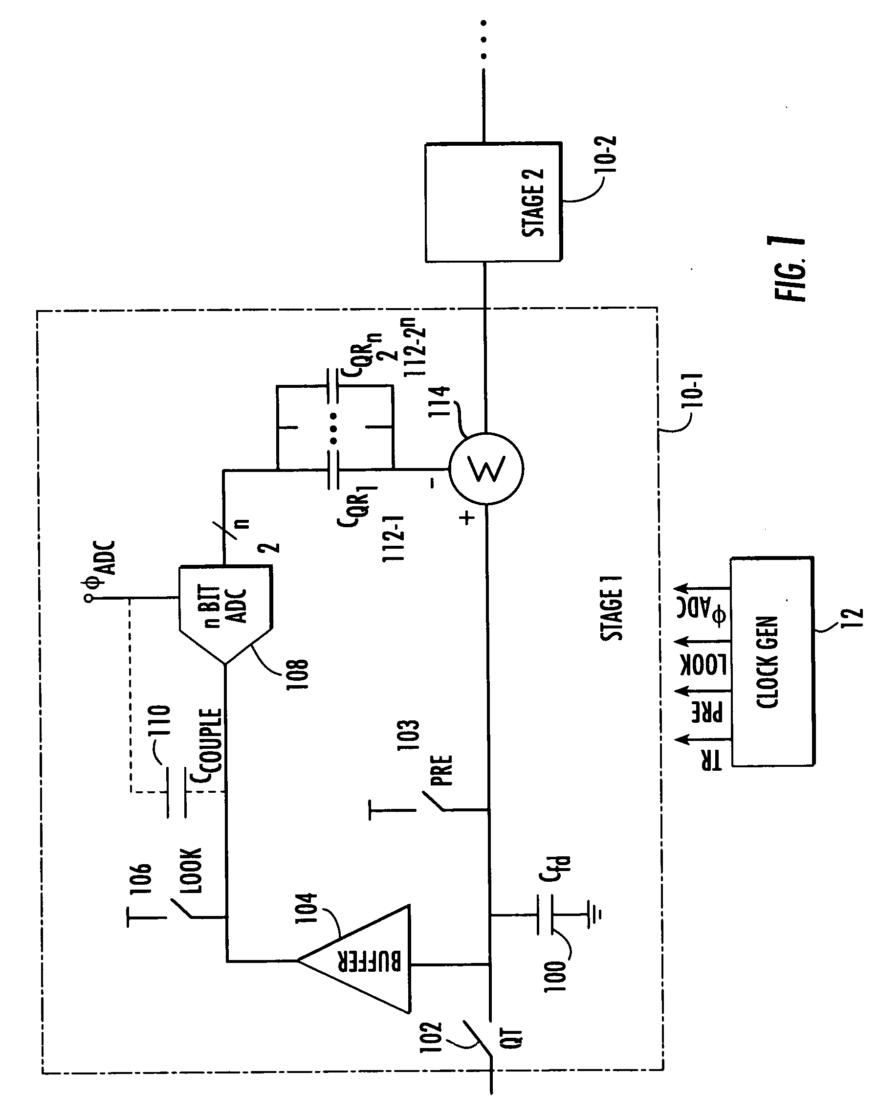
[0016]FIG. 1 is a high level block diagram of a charge pipeline circuit. The specific circuit shown is an Analog to Digital converter (ADC) function comprised of a number of stages 10-1, 10-2, . . . An example stage 10-1 consists of a floating diffusion represented by capacitor 100 (Cfd), a charge transfer input circuit 102, a floating diffusion (FD) pre-charge circuit 103, and a charge output circuit 114. In operation, the pre-charge circuit 103 sets an initial state (voltage) for diffusion 100. An input signal charge (QT) is then fed to the floating diffusion 100 by input circuit 102. A clock signal generator 12 provides the various signals necessary to operate the stages 10 such as an input transfer signal (TR) that controls input circuit 102, a pre-charge signal (PRE) that controls precharge 103, and other signals.

[0017]Introduction of this charge to the floating diffusion causes the voltage thereon to change. I...


PUM


Abstract

A technique for operating a source follower buffer circuit, such as employed in a charge domain pipeline, to eliminate floating diffusion signal charge contamination from downstream circuits. The method and apparatus places an output of the circuit in a known state immediately prior to charge transfer into a floating diffusion, and again in known state immediately prior to charge transfer out of the floating diffusion.

Description

RELATED APPLICATION(S)[0001]This application claims the benefit of U.S. Provisional Application No. 61 / 005,773, filed on Dec. 7, 2007. The entire teachings of the above application(s) are incorporated herein by reference.BACKGROUND OF THE INVENTION[0002]In charge domain pipeline circuits, such as used in Analog to Digital Converters (ADCs) and other applications, signal charge is transferred from a sending capacitive net to a pre-charged receiving capacitive net using a charge transfer device. These capacitive nets are typically implemented as floating diffusions. Transfer of a signal charge into a capacitive net causes the voltage on the capacitive net to drop from a pre-charged voltage by an amount proportional to the amount of charge.[0003]In order to measure the size of the signal charge, as needed for the purpose of comparing it to another charge packet on an opposing floating diffusion of a differential design, it is necessary to either amplify or buffer the change in voltage....

Claims


Application Information

Patent Timeline
Patent Type & Authority Applications(United States)
IPC IPC(8): H03B1/00
CPCH03M1/168G11C27/026
Inventor WASHKURAK, WILLIAM D.
Owner INTERSIL INC
Learn More