Charge pump circuit
a pump circuit and pump technology, applied in the direction of pulse generators, pulse techniques, instruments, etc., can solve the problems of increased production cost, product bulkyness, increased production cost, etc., and achieve the effect of reducing the number of stabilizing capacitors and high output voltag
- Summary
- Abstract
- Description
- Claims
- Application Information
AI Technical Summary
Benefits of technology
Problems solved by technology
Method used
Image
Examples
first embodiment
[0032]FIG. 5 is a circuit diagram of a charge pump according to a first embodiment of the present invention. Referring to FIG. 5, there is shown a charge pump circuit 500 including a first switch SW1, a second switch SW2, a third switch SW3, a fourth switch SW4, a fifth switch SW5, a sixth switch SW6, a fly capacitor Cf2, and an output capacitor Cout.
[0033]The pump unit 510 includes a first terminal T1, a second terminal T2, a third terminal T3, and a fourth terminal T4. The first terminal T1 of the pump unit 510 is coupled to an input voltage Vin, and the second terminal T2 of the pump unit 510 is coupled to a first voltage V1, i.e., a grounding voltage GND. The pump unit 510 further includes an internal capacitor Cf1, a seventh switch SW7, and an eighth switch SW8. The seventh switch SW7 includes a first terminal and a second terminal. The internal capacitor Cf1 includes a first terminal and a second terminal. The first terminal of the seventh switch SW7 is coupled to the first te...
second embodiment
[0040]FIG. 7 is a circuit diagram of a charge pump according to a second embodiment of the present invention. Referring to FIG. 7, there is shown a charge pump circuit 700. The charge pump circuit 700 includes a pump unit 710, a first switch SW1, a second switch SW2, a third switch SW3, a fourth switch SW4, a fifth switch SW5, a sixth switch SW6, a fly capacitor Cf2, and an output capacitor Cout.
[0041]The first switch SW1 includes a first terminal and a second terminal. The first terminal of the first switch SW1 is coupled to a second voltage V2, e.g., an input voltage Vin. The second terminal of the first switch SW1 is coupled to the third terminal T3 of the pump unit 710. The second switch SW2 includes a first terminal and a second terminal. The first terminal of the second switch SW2 is coupled to the fourth terminal T4 of the pump unit 710. The third switch SW3 includes a first terminal and a second terminal. The first terminal of the third switch SW3 is coupled to the second te...
third embodiment
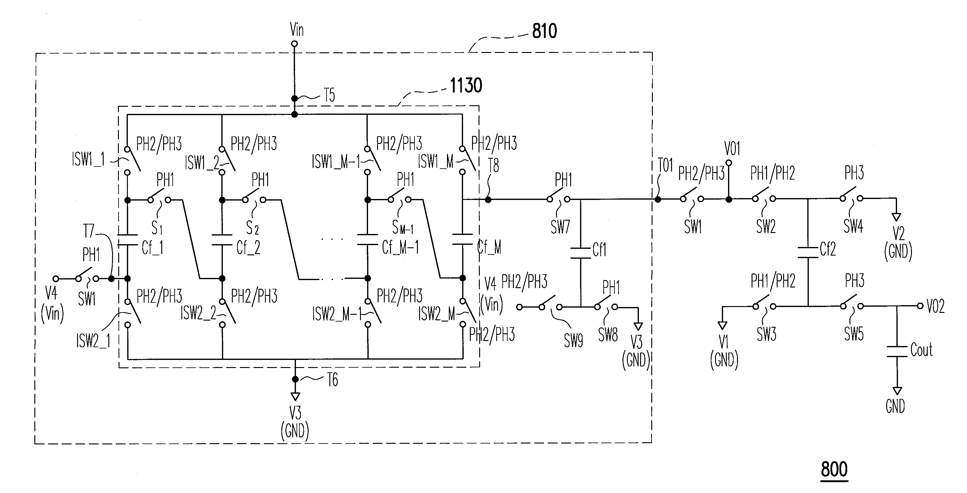
[0049]FIG. 8 is a circuit block diagram of a charge pump according to a third embodiment of the present invention. Referring to FIG. 8, there is shown a charge pump circuit 800. The charge pump circuit 800 includes a pump unit 810, a first switch SW1, a second switch SW2, a third switch SW3, a fourth switch SW4, a fifth switch SW5, a fly capacitor Cf2, and an output capacitor Cout. The pump unit 810 includes an input terminal and an output terminal TO1. The input terminal of the pump unit 810 receives an input voltage Vin, and a first output voltage VO1 is provided from the output terminal TO1 of the pump unit 810.
[0050]The first switch SW1 includes a first terminal and a second terminal. The first terminal of the first switch SW1 is coupled to the output terminal TO1 of the pump unit 810. The second terminal of the first switch SW1 is coupled to the output terminal of the first output voltage VO1. The second switch SW2 includes a first terminal and a second terminal. The first term...
PUM
 Abstract
Description
Claims
Application Information
 - R&D
- Intellectual Property
- Life Sciences
- Materials
- Tech Scout
- Unparalleled Data Quality
- Higher Quality Content
- 60% Fewer Hallucinations
Browse by: Latest US Patents, China's latest patents, Technical Efficacy Thesaurus, Application Domain, Technology Topic, Popular Technical Reports.
© 2025 PatSnap. All rights reserved.Legal|Privacy policy|Modern Slavery Act Transparency Statement|Sitemap|About US| Contact US: help@patsnap.com


