Storage controller for flash memory including a crossbar switch connecting a plurality of processors with a plurality of internal memories

Active Publication Date: 2009-07-02
SANDISK TECH LLC
View PDF102 Cites 202 Cited by
  • Summary
  • Abstract
  • Description
  • Claims
  • Application Information

AI Technical Summary

Benefits of technology

[0011]In one embodiment, the described solution to the performance limitations of flash memory involves the use of multiple microprocessors in the controller design, thereby creating multiple parallel independent pipelines, each of which is capable of handling a portion of a single transaction. This design maximizes use of the host and flash interfaces, and allows individual transactions to be broken up into many small portions, which can be reordered and handled in parallel to increase performance. The architecture is designed to allow multiple processors to perform their functions without the use of costly and inefficient interrupts.

Problems solved by technology

Nevertheless, flash memory has not traditionally been used in such environments due to certain technical constraints.
The first technical problem is write speed, which may be as slow as one-tenth that of a mechanical hard drive.
This results from the fact that data cannot be overwritten on a NAND flash device without a long erase cycle prior to the write.
Because the erase cycle directly affects the write performance, most flash designs move the write data to a new location and delay the erase until later.
In a busy system, delayed erase cycles may build up until the processor runs out of free flash pages and has to stop to create new ones, thereby significantly affecting system performance.
The second technical problem is the specified limit for each flash memory page of 100,000 erase cycles for Single Level Cell (“SLC”) devices and 10,000 cycles for Multi-Level Cell (“MLC”) devices.
These pose particular problems for datacenters that operate with unpredictable data streams that may cause “hot spots,” resulting in certain highly-used areas of memory being subject to a large number of erases.

Method used


Image

  • Storage controller for flash memory including a crossbar switch connecting a plurality of processors with a plurality of internal memories
  • Storage controller for flash memory including a crossbar switch connecting a plurality of processors with a plurality of internal memories
  • Storage controller for flash memory including a crossbar switch connecting a plurality of processors with a plurality of internal memories

Examples


Embodiment Construction

I. Overview.

[0071]A. System Overview.

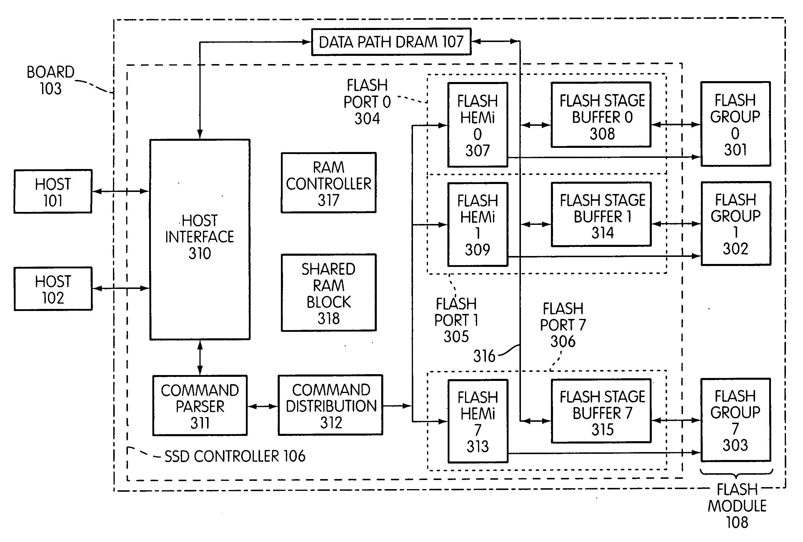
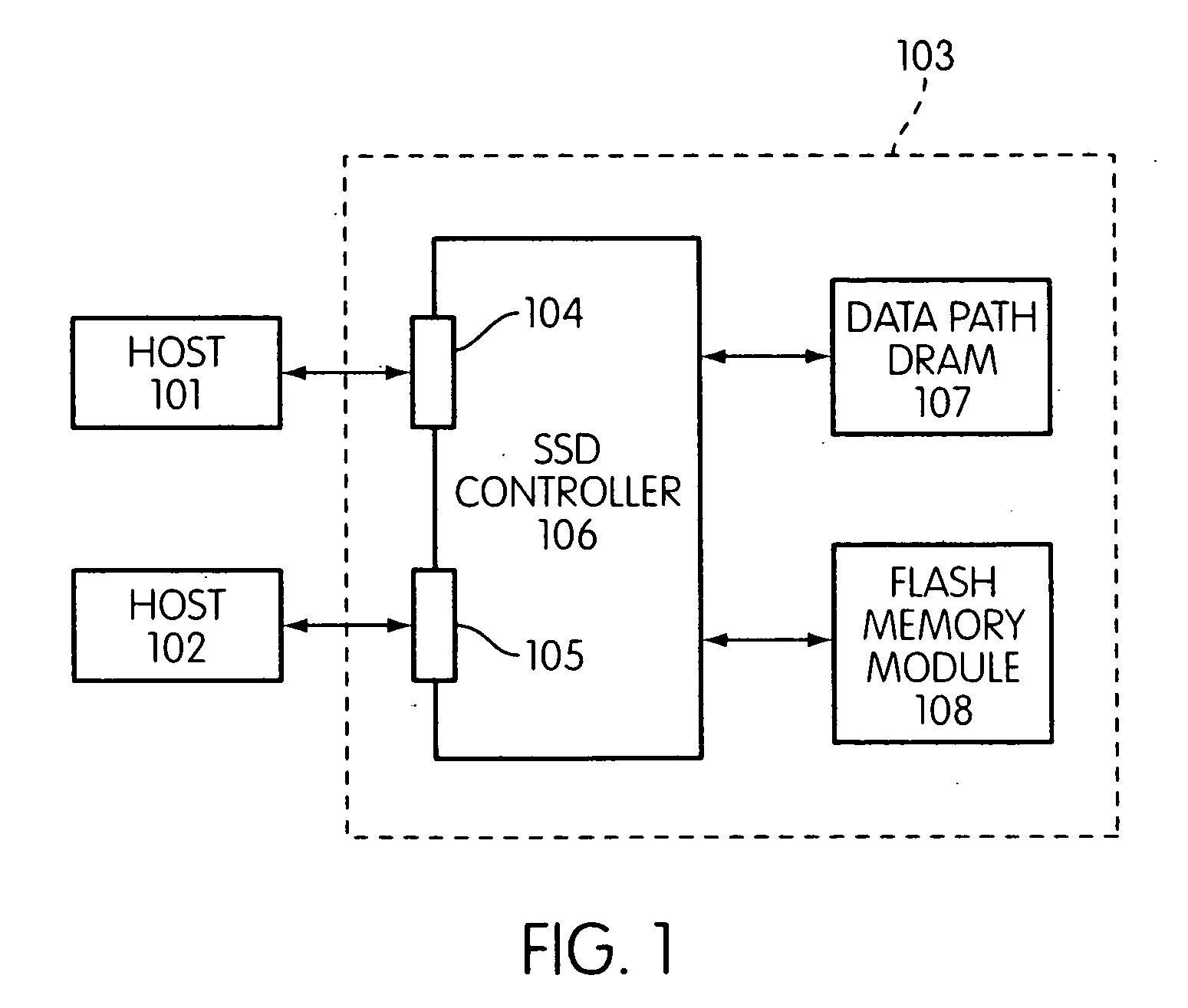
[0072]In the currently preferred embodiment, the system described herein is designed to operate with various enterprise-level mass storage protocols, including SAS (“Serial Attached SCSI”), FC (“Fibre Channel”) and FC-AL (“Fibre Channel Arbitrated Loop), all of which are based on the Small Computer Systems Interface (“SCSI”), and Serial ATA (“SATA”) protocols. These protocols are highly familiar to those of ordinary skill in the art, and will not be further described herein. Except where particular protocols are called out, the systems and methods disclosed herein do not depend on the particular protocol being used and are designed to operate correctly with all of them. Moreover, these systems and methods may be adapted for use with other similar protocols, either currently in use or not yet developed, including protocols designed for enterprise-level applications as well as protocols designed for other applications, such as end-user.
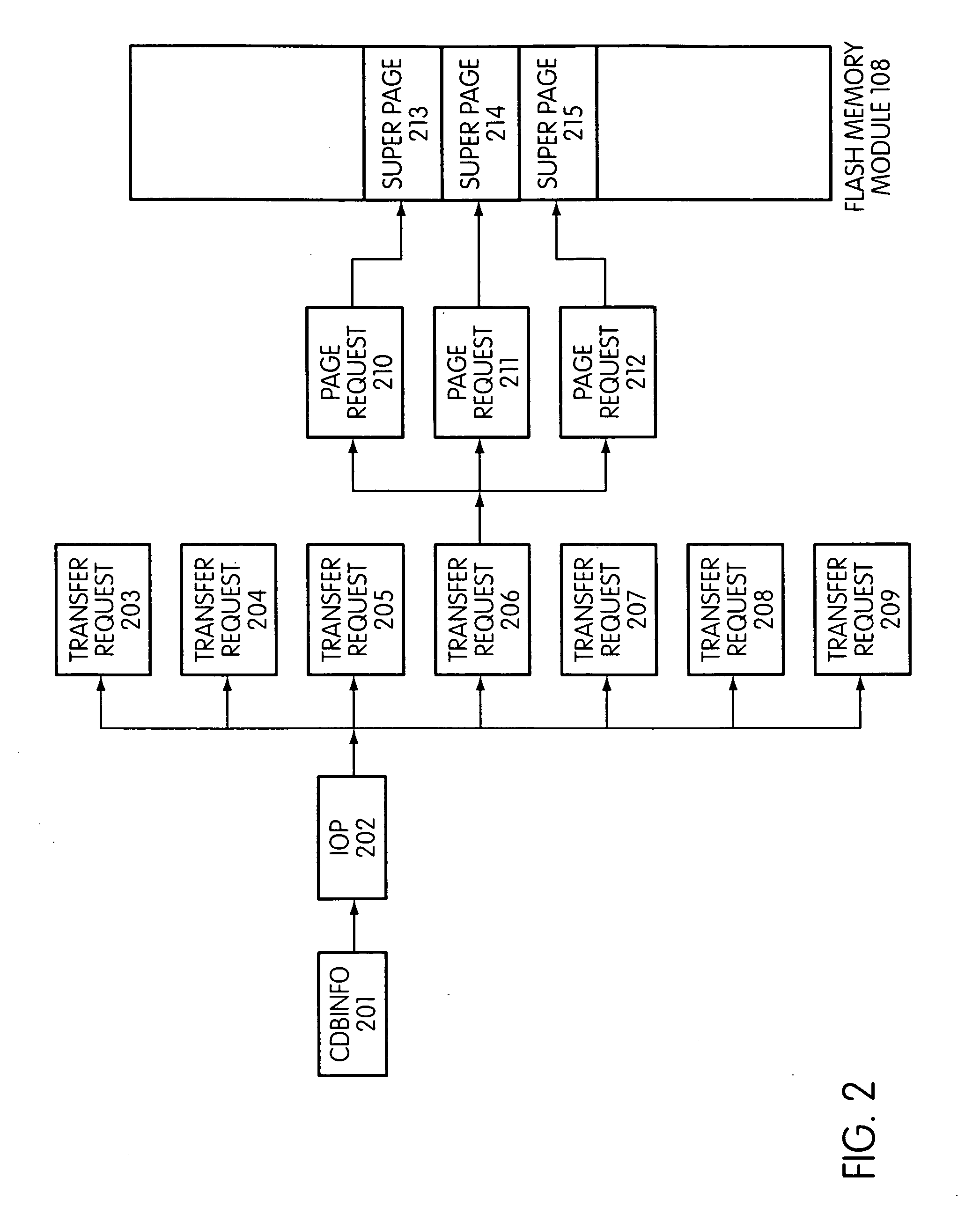
[0073]As a m...


PUM


Abstract

A controller designed for use with a flash memory storage module, including a crossbar switch designed to connect a plurality of internal processors with various internal resources, including a plurality of internal memories. The memories contain work lists for the processors. In one embodiment, the processors communicate by using the crossbar switch to place tasks on the work lists of other processors.

Description

CROSS-REFERENCE TO RELATED APPLICATIONS[0001]This application claims priority to U.S. Provisional Patent Application No. 61 / 017,123 filed Dec. 27, 2007, the disclosure of which is incorporated herein by reference, as if fully stated here, for all purposes.[0002]The present application contains subject matter related to the subject matter in the following copending patent applications: U.S. patent application Ser. No. M-17228-01 US filed on even date herewith and entitled “System and Method for Performing Host Initiated Mass Storage Commands Using a Hierarchy of Data Structures;” U.S. patent application Ser. No. M-17228-02 US, filed on even date herewith and entitled “Flash Memory Controller Having Reduced Pinout;” U.S. patent application Ser. No. M-17228-03 US, filed on even date herewith and entitled “Multiprocessor Storage Controller;” U.S. patent application Ser. No. M-17228-05 US, filed on even date herewith and entitled “Flash Memory Controller and System Including Data Pipelin...

Claims


Application Information

Patent Timeline
IPC IPC(8): G06F12/00
CPCG06F13/1657G11C7/1051G06F2212/7201G11C16/10G06F12/0246G11C7/1063G06F3/0604G06F3/0659G06F3/0679G06F13/28G06F2212/7203G06F2212/7205
Inventor PRINS, DOUGLAS A.OLBRICH, AARON K.
Owner SANDISK TECH LLC
Why Eureka
Try Eureka