
Solid-state image pickup device and drive method thereof

Inactive Publication Date: 2009-05-28
PANASONIC CORP
View PDF8 Cites 0 Cited by
  • Summary
  • Abstract
  • Description
  • Claims
  • Application Information

AI Technical Summary

Benefits of technology

[0015]The present invention is proposed in view of the above circumstances and the purpose of the present invention is to provide a solid-state image pickup device having a reduced number of terminals and a solid-state image pickup device drive method capable of reducing the number of terminals.
[0017]The solid-state image pickup device uses a common terminal as a vertical transfer signal input terminal and as a horizontal transfer signal input terminal; therefore, the solid-state image pickup device has a reduced number of terminals. In other words, the number of electrode pads formed on the chip of the solid-state image pickup device can be reduced. Consequently, the chip can have a reduced area and an ultracompact solid-state image pickup device can be realized.
[0020]The present invention can reduce the number of terminals (number of electrode pads) that is a determination factor of the chip size of a solid-state image pickup device; therefore, the solid-state image pickup device can be downsized. Particularly, small solid-state image pickup devices mounted in endoscopes can significantly be downsized, leading to magnificent efficacy in practice.

Problems solved by technology

It is difficult to extremely reduce the electrode pads in size because they are used for wire bonding to make electric connection to the external terminals of a package in which the semiconductor integrated circuit device is sealed.
It is also difficult to extremely reduce the distance between electrode pads.
However, the prior art structure does not allow the solid-state image pickup device to be downsized because an area for providing ten terminals as described above has to be ensured on the chip.

Method used


Image

  • Solid-state image pickup device and drive method thereof
  • Solid-state image pickup device and drive method thereof
  • Solid-state image pickup device and drive method thereof

Examples


Embodiment Construction

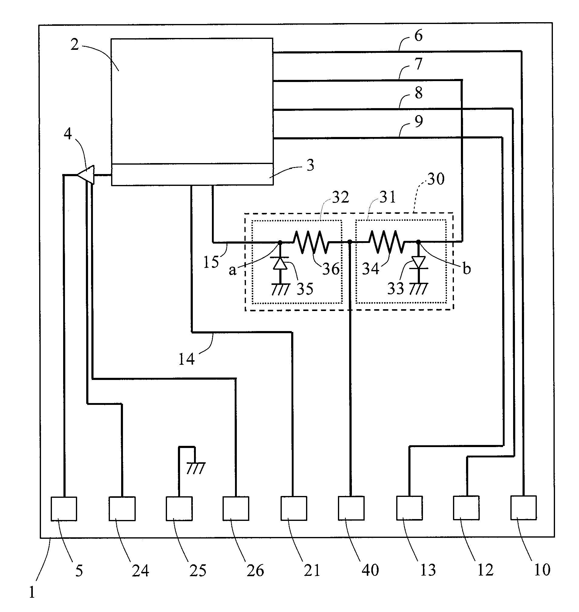
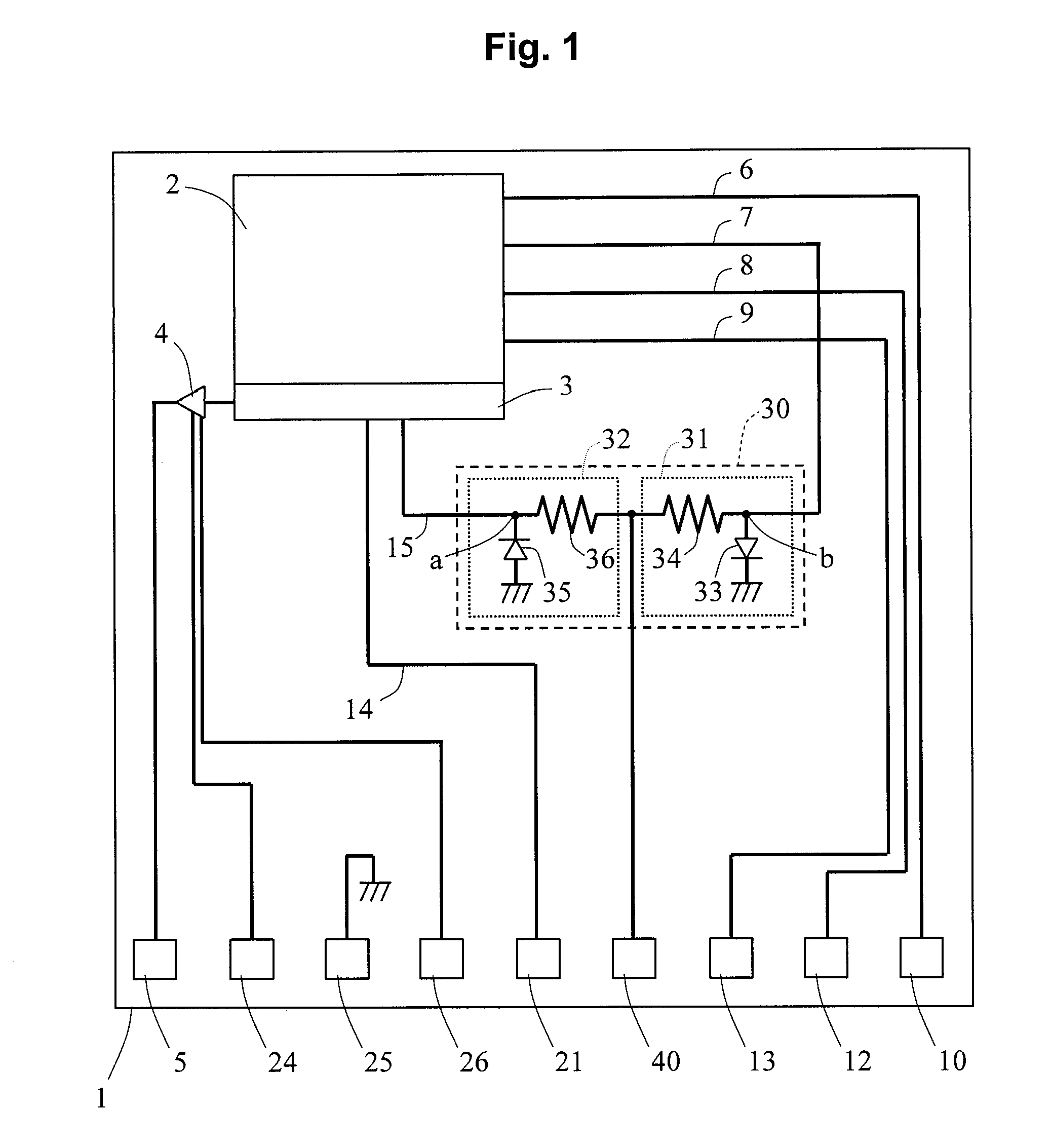
[0026]An embodiment of the present invention will be described in detail hereafter with reference to the drawings. In the embodiment below, the present invention is realized as a CCD-type solid-state image pickup device having vertical transfer parts of a four-phase drive type and a two-phase drive type horizontal transfer part.

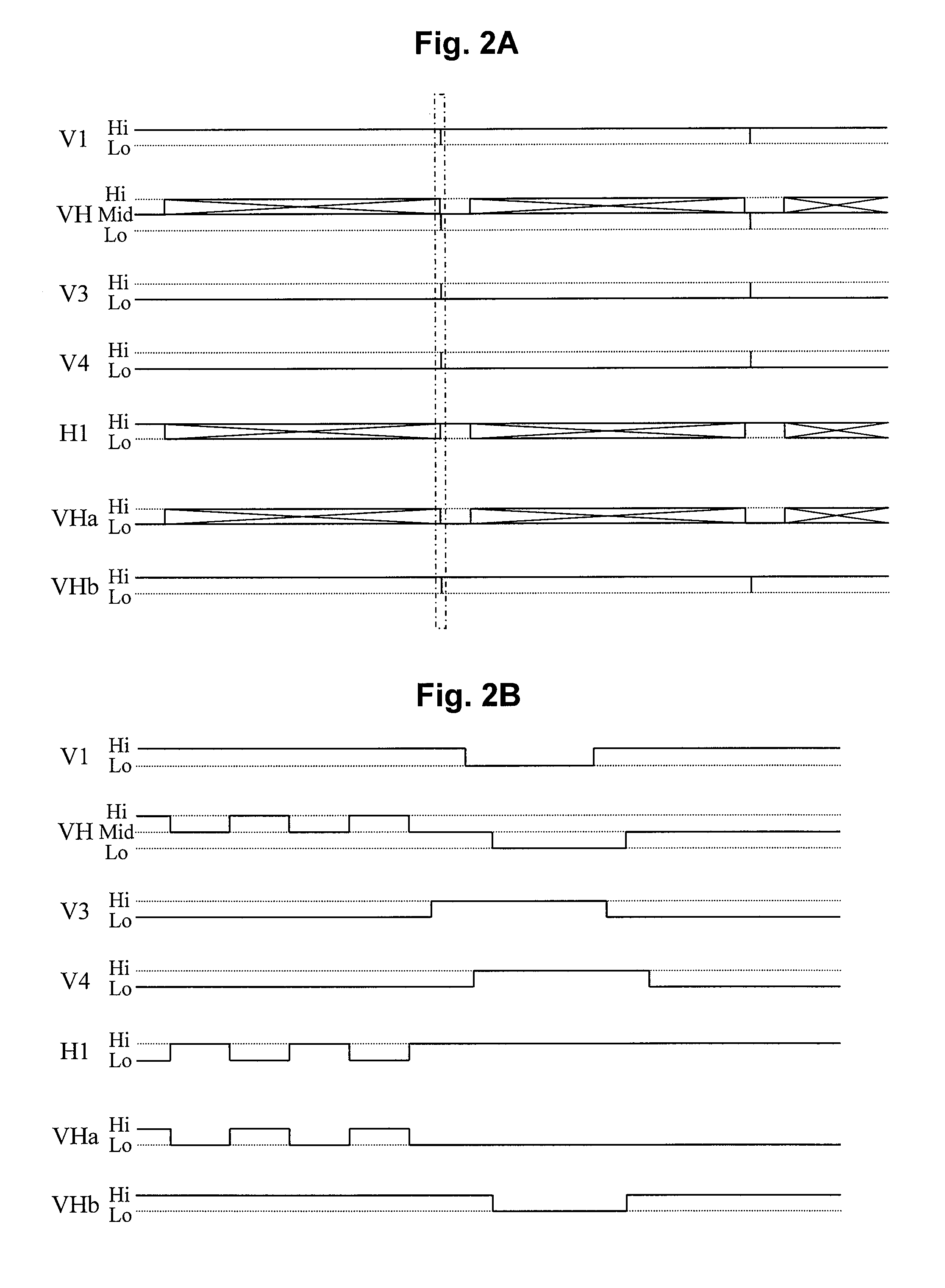
[0027]FIG. 1 is a diagrammatic plane view showing the structure of the solid-state image pickup device according to an embodiment of the present invention. As shown in FIG. 1, a solid-state image pickup device 1 of this embodiment comprises a pixel area (pixel part) 2 where received light is converted to electric signals through photoelectric conversion. Multiple pixels are two-dimensionally arranged in the pixel area 2. Each pixel has a photodiode generating signal charge according to incident light. Vertical transfer parts (vertical CCDs) for vertically (the up-and-down direction in FIG. 1) transferring the signal charges generated at the pixels are provide...


PUM


Abstract

A solid-state image pickup device relating to the present invention comprises a pixel area where multiple pixels used for photoelectric conversion of incident light are two-dimensionally arranged. Vertical signal input lines to which vertical transfer signals for transferring signal charges generated at the pixels vertically in the pixel area are applied are connected to the pixel area. Furthermore, horizontal signal input lines to which horizontal transfer signals for horizontally transferring the signal charges are applied are connected to a horizontal transfer part for horizontally transferring the signal charges transferred vertically in the pixel area. A signal separation part separates vertical and horizontal transfer signals from a pulse signal supplied via a complex signal input terminal and supplies the separated signals to the vertical signal input line and the horizontal signal input line, respectively.

Description

CROSS-REFERENCE TO RELATED APPLICATION[0001]The present application claims the benefit of patent application number 2007-307255, filed in Japan on Nov. 28, 2007, the subject matter of which is incorporated herein by reference.BACKGROUND OF THE INVENTION[0002]1. Field of the Invention[0003]The present invention relates to a solid-state image pickup device applicable to integrated video cameras and digital still cameras and a drive method thereof.[0004]2. Description of the Related Art[0005]Recently, solid-state image pickup devices have been extensively used in the image pickup part of integrated video cameras. Particularly, CCD (charge coupled device) solid-state image pickup devices having excellent noise properties have been extensively used (for example, reference Japanese Laid-Open Patent Application Publication No. H04-180265).[0006]FIG. 3 is a diagrammatic plane view showing a structure of a prior art solid-state image pickup device. As shown in FIG. 3, prior art solid-state i...

Claims


Application Information

Patent Timeline
IPC IPC(8): H04N5/335H04N5/341H04N5/372H04N5/378
CPCH04N5/372H04N5/335H04N25/00H04N25/71H04N23/10H04N25/75
Inventor MATSUDA, YUJI
Owner PANASONIC CORP
Learn More