Susceptor for epitaxial layer forming apparatus, epitaxial layer forming apparatus, epitaxial wafer, and method of manufacturing epitaxial wafer
- Summary
- Abstract
- Description
- Claims
- Application Information
AI Technical Summary
Benefits of technology
Problems solved by technology
Method used
Image
Examples
examples
[0076]A P-type silicon wafer which is doped with P-type dopant and is 150 mm in diameter was prepared, and an epitaxial layer was formed on the P-type silicon wafer in the following procedures.
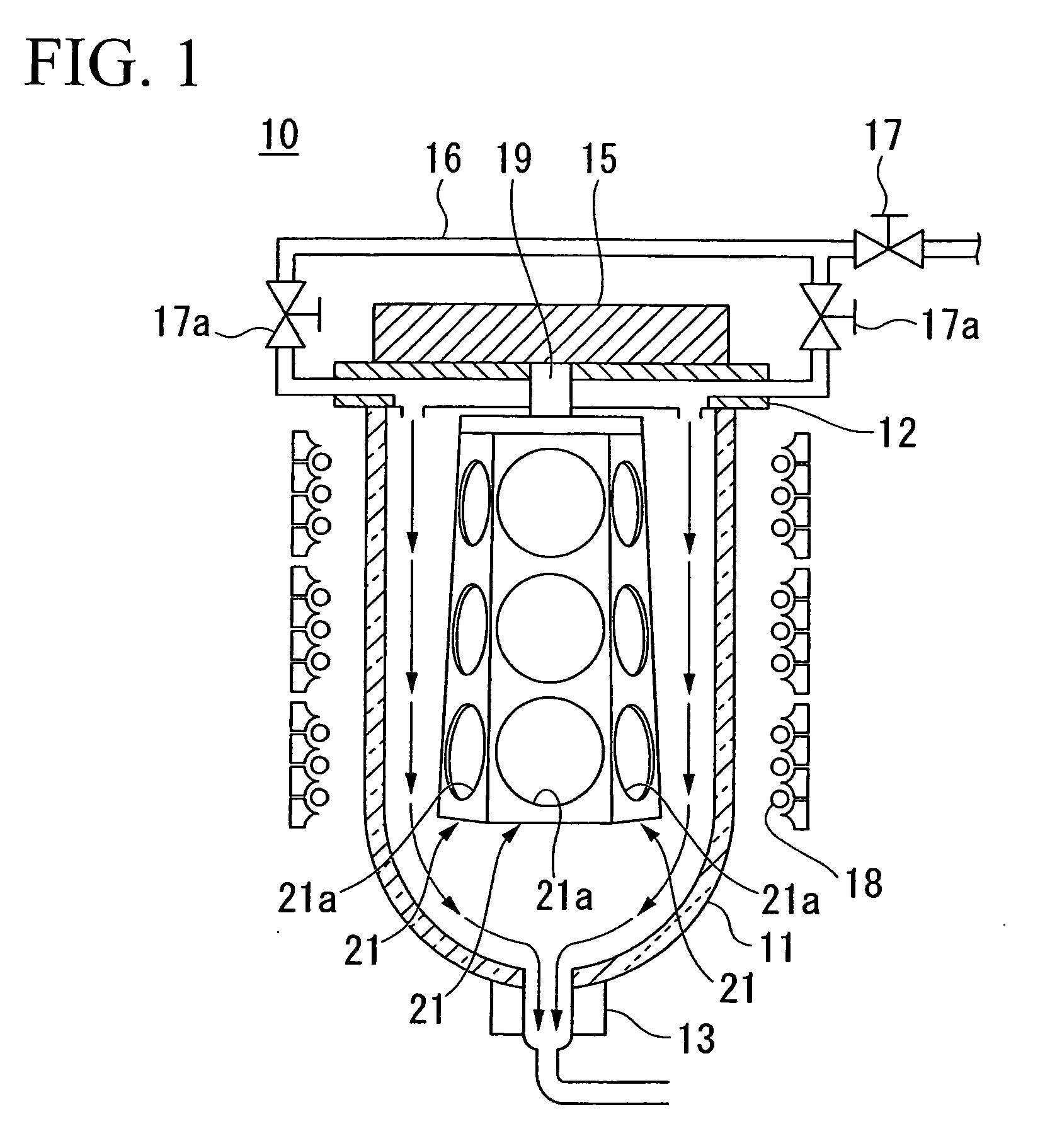
[0077]The epitaxial layer forming apparatus shown in FIG. 1 was prepared, and the P-type silicon wafer was accommodated in a recessed portion of a susceptor of the apparatus. Then, hydrogen gas was purged inside a bell jar, and the P-type silicon wafer was heated uniformly by raising the inside of the bell jar up to a temperature of 1220° with the heater while rotating the susceptor.
[0078]Then, an epitaxial layer having a thickness of 9 μm was grown by supplying reaction gas, which is obtained by adding silicon source gas of TCS (trichlorosilane) to hydrogen gas with a concentration rate of 5%, inside the bell jar by a flow rate of 150 ml / min.
[0079]Moreover, in the above process, the diameter of the recessed portion of the susceptor was set to about 150 mm, the width of the groove was set to 2...
PUM
| Property | Measurement | Unit |
|---|---|---|
| Height | aaaaa | aaaaa |
| Height | aaaaa | aaaaa |
| Height | aaaaa | aaaaa |
Abstract
Description
Claims
Application Information
 - R&D
- Intellectual Property
- Life Sciences
- Materials
- Tech Scout
- Unparalleled Data Quality
- Higher Quality Content
- 60% Fewer Hallucinations
Browse by: Latest US Patents, China's latest patents, Technical Efficacy Thesaurus, Application Domain, Technology Topic, Popular Technical Reports.
© 2025 PatSnap. All rights reserved.Legal|Privacy policy|Modern Slavery Act Transparency Statement|Sitemap|About US| Contact US: help@patsnap.com


