
Manufacturing Process for a Prepreg with a Carrier, Prepreg with a Carrier, Manufacturing Process for a Thin Double-Sided Plate, Thin Double-Sided Plate and Manufacturing Process for a Multilayer-Printed Circuit Board

a manufacturing process and prepreg technology, applied in the field of manufacturing process of a prepreg with a carrier, a manufacturing process for a multi-layer printed circuit board, can solve the problems of insufficient imprinting of resin components, deterioration of insulation reliability, and insufficient material base material of the fabric base material, and achieve excellent thickness precision

Inactive Publication Date: 2009-05-21
SUMITOMO BAKELITE CO LTD
View PDF9 Cites 27 Cited by
  • Summary
  • Abstract
  • Description
  • Claims
  • Application Information

AI Technical Summary

Benefits of technology

The present invention provides a process for manufacturing a prepreg with carriers that have excellent thickness precision and can be used for preparing a multilayer-printed circuit board. The process involves laminating an insulating resin layer onto a textile fabric base material and heating it to bond it. The resulting prepreg has residual voids, which can deteriorate insulation reliability when used in a multilayer-printed circuit board. The invention also provides a process for manufacturing a thin double-sided plate and a thin double-sided package using the prepreg. The prepreg can be made with carriers that have a larger dimension than the textile fabric, and it can be peeled off from the textile fabric. The invention also provides a process for manufacturing a prepreg with carriers that have a film or metal foil insulating resin layer. The resulting prepreg has excellent impregnating properties and can be used for preparing a multilayer-printed circuit board.

Problems solved by technology

In the process, the textile fabric base material is, however, insufficiently impregnated with a resin component, often giving a prepreg with residual voids.
Thus, when such a prepreg is used in manufacturing a multilayer-printed circuit board, insulation reliability may be deteriorated.

Method used


Image

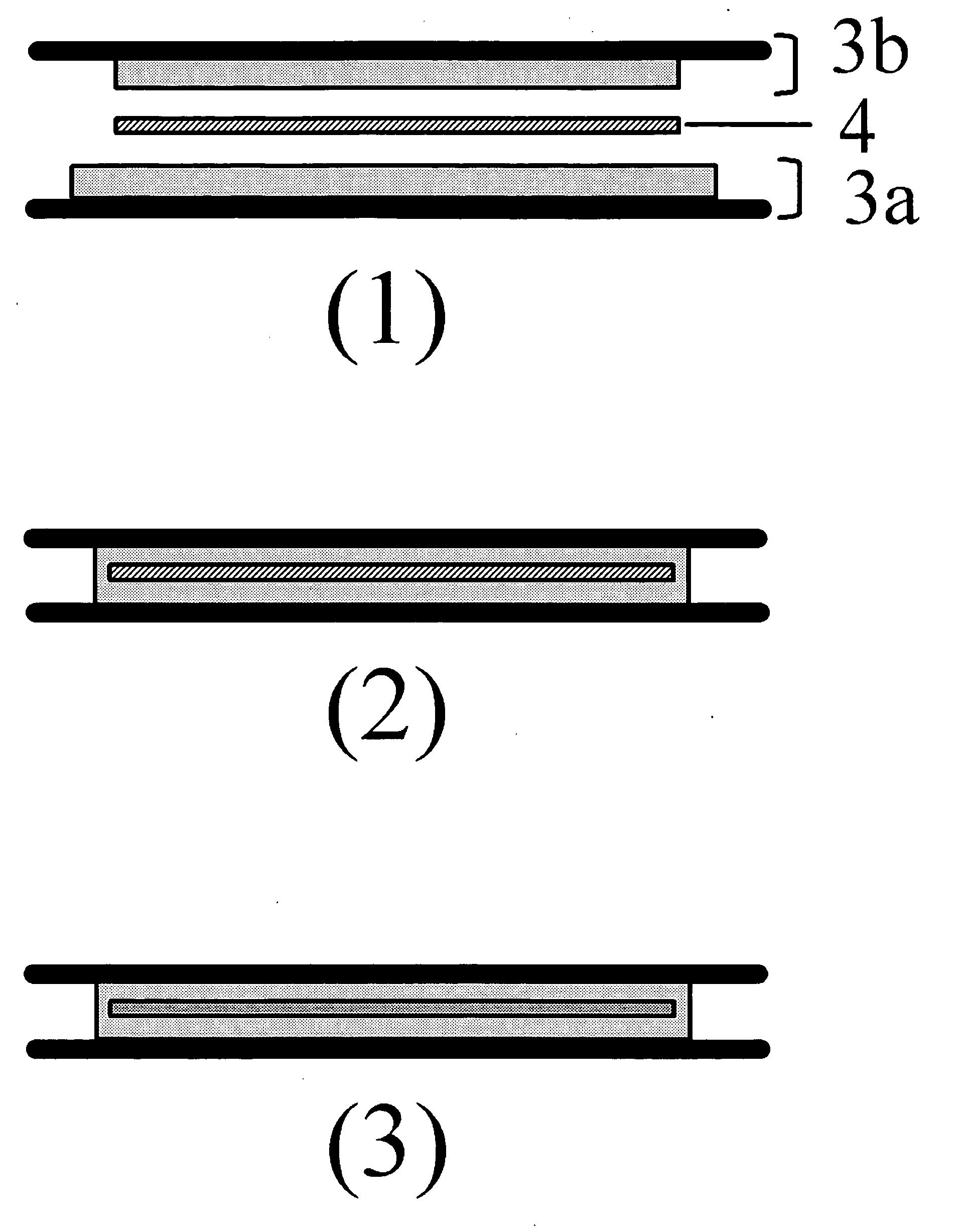
  • Manufacturing Process for a Prepreg with a Carrier, Prepreg with a Carrier, Manufacturing Process for a Thin Double-Sided Plate, Thin Double-Sided Plate and Manufacturing Process for a Multilayer-Printed Circuit Board
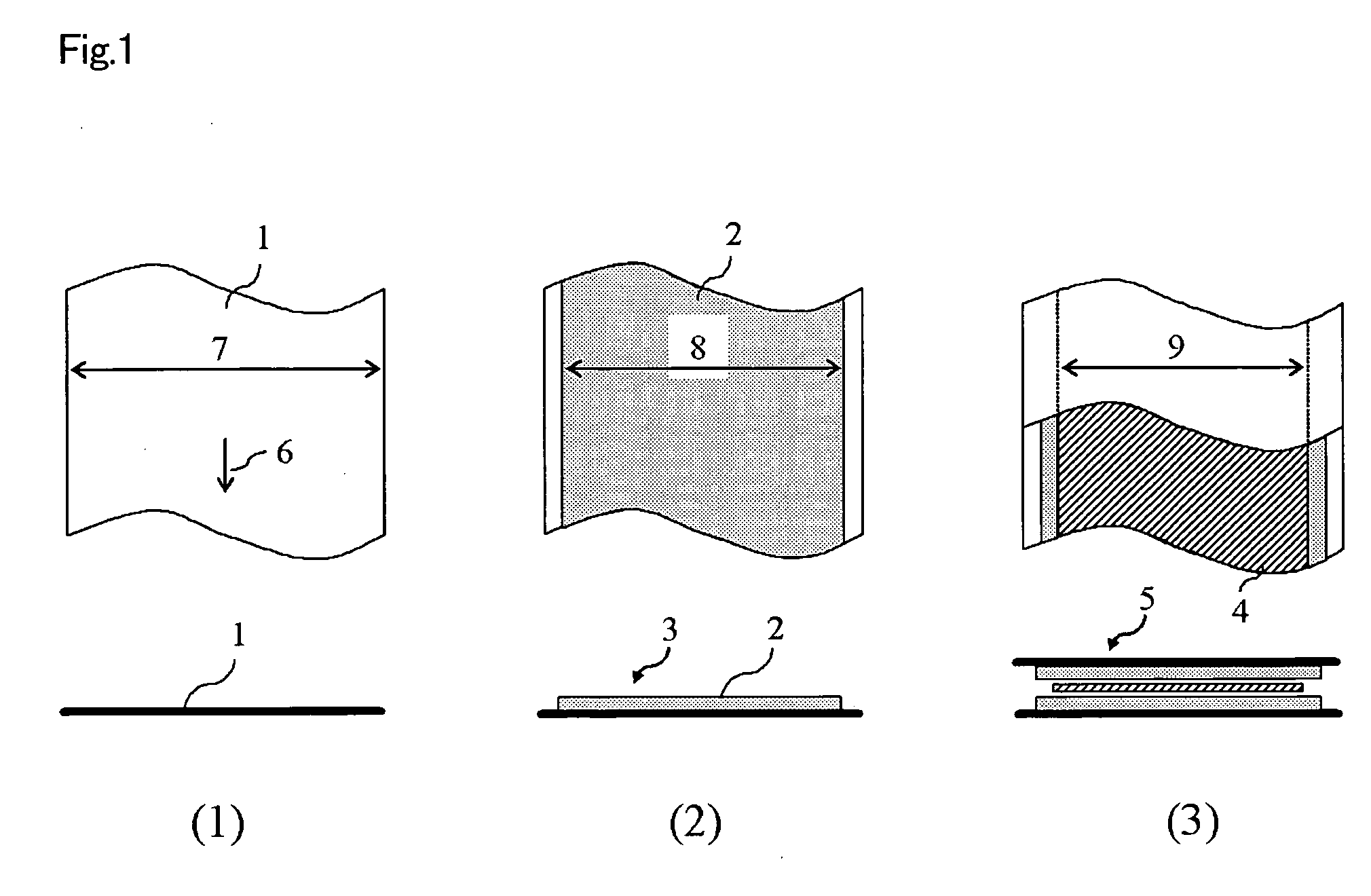
  • Manufacturing Process for a Prepreg with a Carrier, Prepreg with a Carrier, Manufacturing Process for a Thin Double-Sided Plate, Thin Double-Sided Plate and Manufacturing Process for a Multilayer-Printed Circuit Board
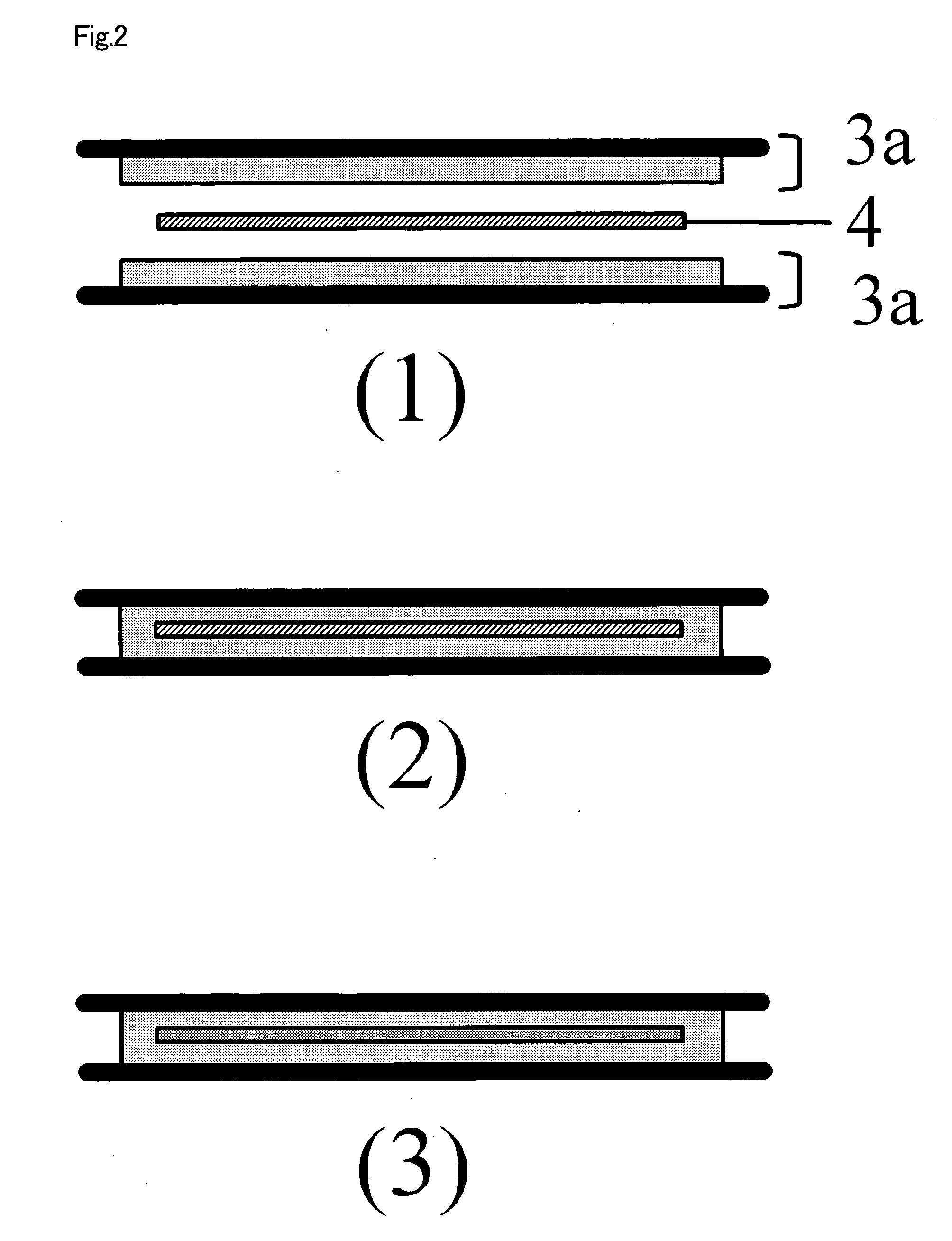
  • Manufacturing Process for a Prepreg with a Carrier, Prepreg with a Carrier, Manufacturing Process for a Thin Double-Sided Plate, Thin Double-Sided Plate and Manufacturing Process for a Multilayer-Printed Circuit Board

Examples


examples

[0339]There will be described the present invention with reference to, but not limited to, experimental examples.

A-1. Preparation of a Liquid Resin Compositional for Forming an Insulating Resin Layer

[0340]In 100 parts by weight of methyl cellosolve were dissolved 100 parts by weight of an epoxy resin (Japan Epoxy Resins Co., Ltd.; “Ep5048”), 2 parts by weight of a curing agent (dicyandiamide) and 0.1 parts by weight of a curing accelerator (2-ethyl-4-methyl imidazole) as resin components, to prepare a resin varnish.

A-2. Preparation of a Carrier with an Insulating Resin Layer

(1) Preparation of a Carrier with an Insulating Resin Layer A1

[0341]A polyethylene terephthalate film with a thickness of 35 μm and a width of 480 mm was used as a carrier.

[0342]Using an apparatus shown in FIG. 5(1), on the carrier was applied the liquid resin compositional prepared above by a comma coater, and then dried in an oven at 170° C. for 3 min, to form a film consisting of an insulating resin layer with...

experimental example a1

[0347]A glass fabric (Unitica Glass Fiber Co., Ltd.; “E02Z-SK”, width: 360 mm, grammage: 17 g / m2) was used as a textile fabric.

[0348]Two carriers with an insulating resin layer A1 prepared above were used as a first and a second carriers with an insulating resin layer.

[0349]Using the apparatus as shown in FIG. 5(2), while the protecting films of the first and the second carriers with an insulating resin layer were peeled, the insulating resin layer sides of the carriers with an insulating resin layer were laminated on both sides of the textile fabric, such that the textile fabric was placed at the center of the carrier in the width direction. They were bonded using laminate rolls (24) at 80° C. under a pressure reduced by 750 Torr.

[0350]Here, in the inner region of the textile fabric in the width-directional dimension, the insulating resin layer sides of the first and the second carriers with an insulating resin layer were bonded to both sides of the textile fabric, and in the outer...

experimental example a2

[0352]As a textile fabric the same textile fabric as in Experimental Example A1 was employed.

[0353]The carrier with an insulating resin layer A1 prepared above was used as a first carrier with an insulating resin layer and the carrier with an insulating resin layer A2 was used as a second carrier with an insulating resin layer.

[0354]The apparatus as shown in FIG. 5(2) was used. While the protecting films of the first and the second carriers with an insulating resin layer were peeled, the insulating resin layer sides of the carriers with an insulating resin layer were laminated on both sides of the textile fabric, such that the textile fabric was placed at the center of the carrier in the width direction. They were bonded using laminate rolls (24) at 80° C. under a pressure reduced by 750 Torr.

[0355]Here, in the inner region of the textile fabric in the width-directional dimension, the insulating resin layer sides of the first and the second carriers with an insulating resin layer we...


PUM

PropertyMeasurementUnit
thicknessaaaaaaaaaa
thicknessaaaaaaaaaa
pressureaaaaaaaaaa

Abstract

A process for manufacturing a prepreg with a carrier exhibiting excellent impregnating properties and thickness precision, which is particularly suitably used for preparing a build-up type multilayer-printed circuit board is provided. Also, a prepreg with a carrier prepared by the manufacturing process and a process for manufacturing a multilayer-printed circuit board utilizing the prepreg with a carrier are provided. There is provided a process for continuously manufacturing a prepreg with a carrier comprising an insulating resin layer having a backbone material of a textile fabric, (a) laminating the insulating resin layer side of a first and a second carriers comprising an insulating resin layer on one side on the both sides of the textile fabric, respectively, to form a laminate and bonding them under a reduced pressure, and (b) after the bonding, heating the laminate at a temperature equal to or higher than a melting point of the insulating resin.

Description

TECHNICAL FIELD[0001]The present invention relates to a manufacturing process for a prepreg with a carrier, a prepreg with a carrier, and a manufacturing process for a multilayer-printed circuit board. This invention also relates to a process for manufacturing a thin double-sided plate, a thin double-sided plate, and a process for manufacturing a multilayer-printed circuit board having a thin double-sided plate.BACKGROUND ART[0002]Recently, there have been needed high-density, densely mounted, and thinner multilayer-printed circuit boards.[0003]A multilayer-printed circuit board is typically manufactured by a build-up method. In the build-up method, to provide an inner-layer circuit board, a circuit is formed on a metal-foiled laminated plate which is prepared by laminating a prepreg and a metal foil and then pressing the laminate under heating. Then, on both sides of the inner-layer circuit board, an insulating layer, which is so-called build-up materials, and a conductor circuit l...

Claims


Application Information

Patent Timeline
Patent Type & Authority Applications(United States)
IPC IPC(8): B32B37/02B32B5/02H05K1/00
CPCB29C70/506B32B2457/08C08J5/24C08J2363/00H05K1/0366H05K3/4673H05K2203/0264H05K2203/066B29K2105/0872B32B5/022B32B5/024B32B15/08B32B15/20B32B27/12B32B27/281B32B27/32B32B27/36B32B3/04B32B2250/44B32B2255/10B32B2255/26B32B2260/021B32B2260/046B32B2262/02B32B2262/0261B32B2262/0269B32B2262/0276B32B2262/10B32B2262/101B32B2307/306B32B2307/308B32B2307/50B29C70/885Y10T442/20C08J5/244C08J5/249B29B11/16H05K3/46
Inventor YUASA, MAROSHIHOSOMI, TAKESHIARAI, MASATAKA
Owner SUMITOMO BAKELITE CO LTD
Learn More