
Circuitized substrate with internal cooling structure and electrical assembly utilizing same

a technology of circuitized substrates and electrical assemblies, applied in the direction of printed circuit assembling, solid-state devices, insulated cables, etc., can solve the problems of insufficient heat dissipation provided by the insulated metal substrate technology, insufficient heat dissipation, and increased heat generation. , to achieve the effect of improving cooling capabilities

Active Publication Date: 2009-04-30
TTM TECH NORTH AMERICA LLC
View PDF42 Cites 37 Cited by
  • Summary
  • Abstract
  • Description
  • Claims
  • Application Information

AI Technical Summary

Benefits of technology

[0026]It is, therefore, a primary object of this invention to enhance the art of circuitized substrates and the art of electrical assemblies which utilize such substrates.
[0027]It is a further object of this invention to provide a new electrical assembly including a circuitized substrate as defined herein with enhanced cooling capabilities.

Problems solved by technology

Because today's technology often demands the use of many such components, including those required to operate at even greater capacities, increasing amounts of heat are being generated.
One drawback of a heat pipe system such as described in 6,226,178 is that the evaporation region is in contact with the single component or with an auxiliary board on which the component is assembled, but it does not effectively cool the entire printed circuit board on which a plurality of heat generating components are assembled.
However, in some power applications such as a control and distribution box in an automobile, the heat dissipation provided by the insulated metal substrate technology may be insufficient to ensure that a deterioration or malfunction of the circuit does not occur due to thermal fatigue.

Method used


Image

  • Circuitized substrate with internal cooling structure and electrical assembly utilizing same
  • Circuitized substrate with internal cooling structure and electrical assembly utilizing same
  • Circuitized substrate with internal cooling structure and electrical assembly utilizing same

Examples


Embodiment Construction

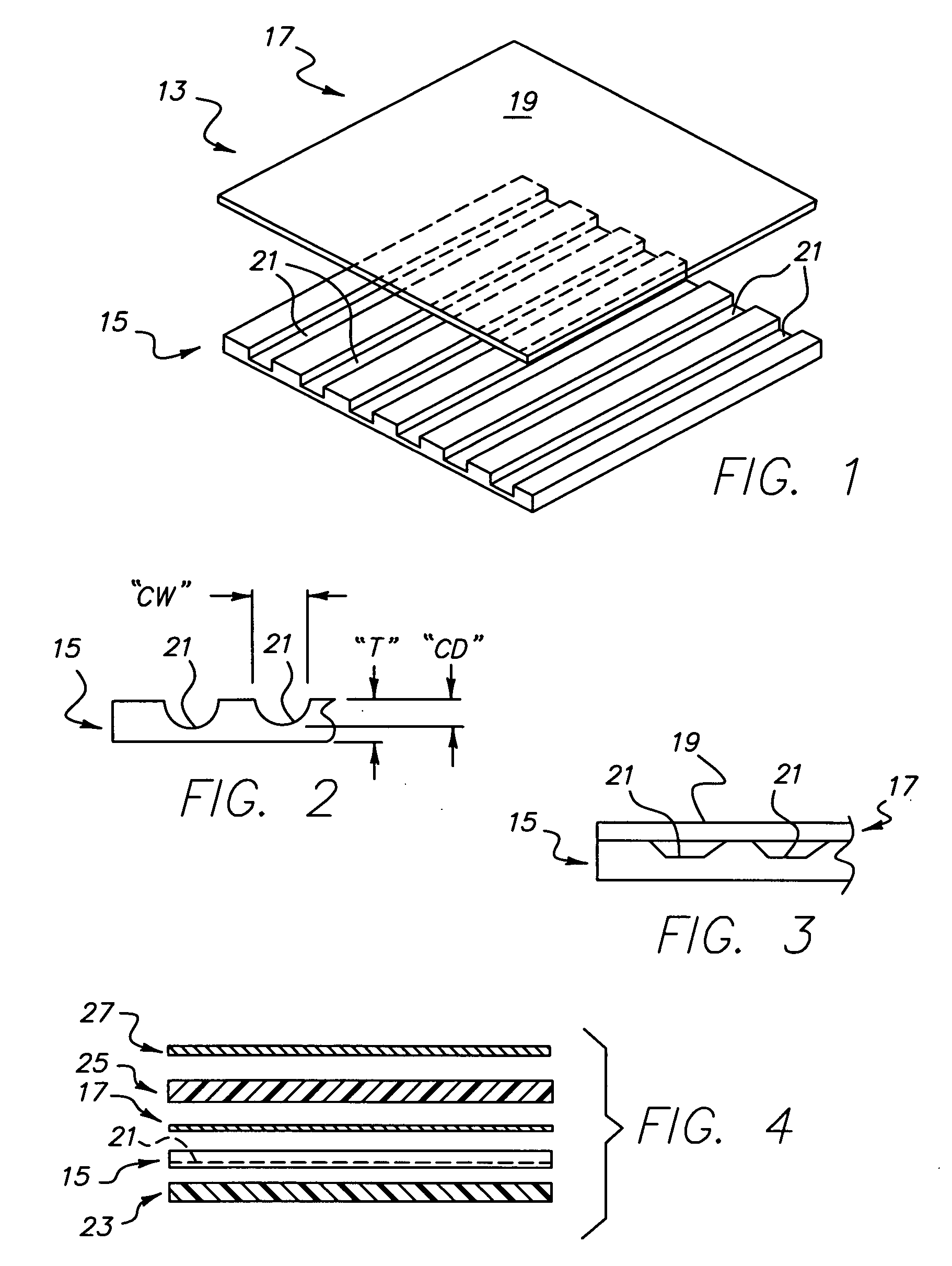
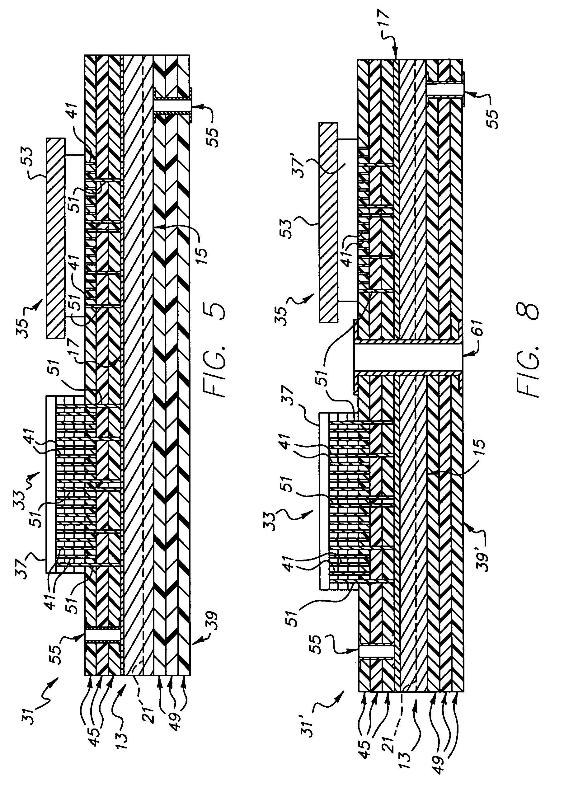
[0039]For a better understanding of the present invention, together with other and further objects, advantages and capabilities thereof, reference is made to the following disclosure and appended claims in connection with the above-described drawings. Like figure numbers may be used from drawing figure to drawing figure to identify like elements in these drawings.

[0040]By the term “circuitized substrate” as used herein is meant to include substrates having at least two (and preferably more) dielectric layers and at least two (and preferably more) metallurgical electrically conductive layers, in addition to at least one thermal cooling structure as part thereof. Examples include structures made of dielectric materials such as fiberglass-reinforced epoxy resins (some referred to as “FR-4” dielectric materials in the art), polytetrafluoroethylene (Teflon), polyimides, polyamides, cyanate resins, photo-imageable materials, and other like materials wherein the conductive layers are each ...


PUM

PropertyMeasurementUnit
Dielectric polarization enthalpyaaaaaaaaaa
Electrical conductivityaaaaaaaaaa
Electrical conductoraaaaaaaaaa

Abstract

An electrical assembly which includes a circuitized substrate including a first plurality of dielectric and electrically conductive circuit layers alternatively oriented in a stacked orientation, a thermal cooling structure bonded to one of the dielectric layers and at least one electrical component mounted on the circuitized substrate. The circuitized substrate includes a plurality of electrically conductive and thermally conductive thru-holes located therein, selected ones of the thermally conductive thru-holes thermally coupled to the electrical component(s) and extending through the first plurality of dielectric and electrically conductive circuit layers and being thermally coupled to the thermal cooling structure, each of these selected ones of thermally conductive thru-holes providing a thermal path from the electrical component to the thermal cooling structure during assembly operation. The thermal cooling structure is adapted for having cooling fluid pass there-through during operation of the assembly. A method of making the substrate is also provided.

Description

TECHNICAL FIELD[0001]The present invention refers to circuitized substrates such as printed circuit boards and chip carriers, and more particularly to such substrates which include internal cooling means as part thereof. The invention further relates to electrical assemblies designed to utilize such substrates.BACKGROUND OF THE INVENTION[0002]One major concern with respect to circuitized substrates adapted for working with electronic components (devices) such as semiconductor chips, modules, resistors etc. involves the effective dissipation of heat generated by such components. In many of today's substrate designs, such components are mounted on one or more external surfaces of the substrate and electrically coupled to selected internal circuitry, e.g., using plated through holes (PTHs). In some more recent products, components such as resistors, capacitors and even semiconductors, are incorporated within the substrate itself. Because today's technology often demands the use of many...

Claims


Application Information

Patent Timeline
IPC IPC(8): H05K7/20H05K3/20
CPCH05K1/0206H05K1/0272H05K3/0061H05K3/44H05K2201/064H05K2201/09745Y10T29/4913H01L2924/0002Y10S428/901H05K2201/10674Y10T29/49126Y10T428/24917H01L2924/00
Inventor CHAN, BENSONEGITTO, FRANK D.LIN, HOW T.MAGNUSON, ROY H.MARKOVICH, VOYA R.THOMAS, DAVID L.
Owner TTM TECH NORTH AMERICA LLC
Learn More