Photonic crystal laser

a laser and photonic crystal technology, applied in the field of laser elements, can solve the problems of difficult to make vcsels capable of moving beams, limit the speed of such mechanical motion, and difficult to accelerate the printing speed in the construction of fig. 1, and achieve the effect of high output power

Active Publication Date: 2009-02-05
KYOTO UNIV +1
View PDF7 Cites 8 Cited by
  • Summary
  • Abstract
  • Description
  • Claims
  • Application Information

AI Technical Summary

Benefits of technology

[0010]One objective of the present invention is to provide a laser element and a laser device where beams o

Problems solved by technology

However, there are limitations to enhance the speed of such a mechanical motion, and it is difficult to accelerate the printing speed in the construction of FIG. 1.
However, it is diffi

Method used


Image

  • Photonic crystal laser
  • Photonic crystal laser
  • Photonic crystal laser

Examples


Embodiment Construction

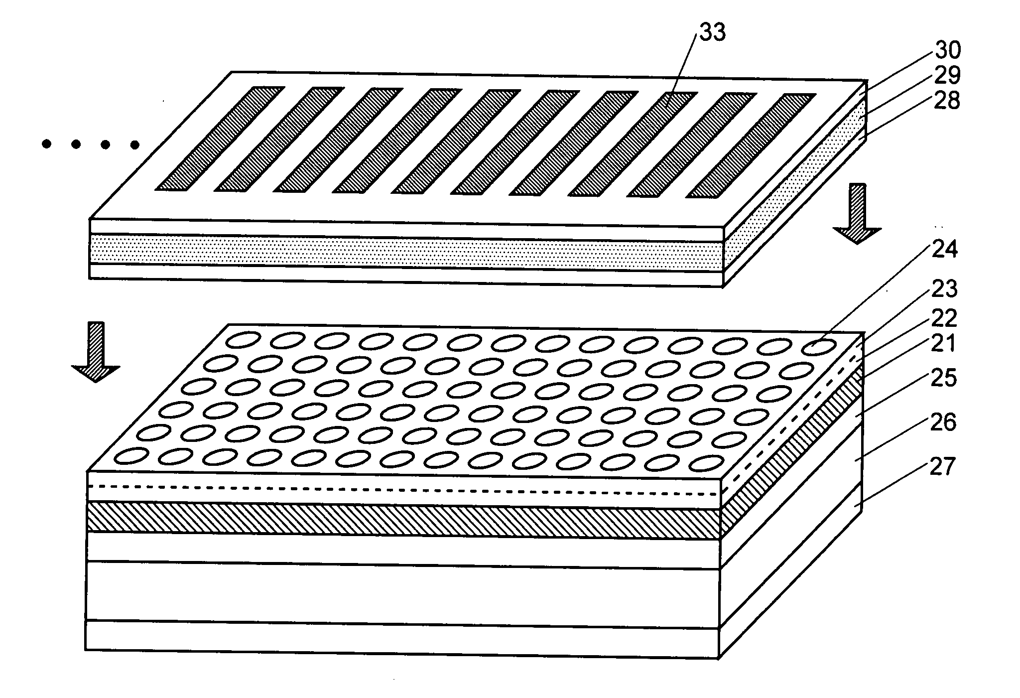
[0070]An embodiment of the photonic crystal laser element according to the present invention is described referring to FIG. 2.

[0071]A two-dimensional photonic crystal 23 is provided on an active layer 21 made of Indium Gallium Arsenide (InGaAs) / Gallium Arsenide (GaAs) and having multiple-quantum wells (MQW) via a lower spacer 22. The two-dimensional photonic crystal 23 includes a plate member made of GaAs and having holes 24 periodically arranged in a square lattice pattern. In the present embodiment, the lower spacer 22 and the two-dimensional photonic crystal layer 23 are created as a single layer, in which the holes 24 are present only in the upper portion thereof in order to function as the two-dimensional photonic crystal layer 23 in the upper portion and function as the lower spacer 22 in the lower portion thereof. On the lower side of the active layer 21, a confining layer 25 made of GaAs, a lower cladding layer 26 made of n-type aluminum gallium arsenide (AlGaAs), and a lowe...


PUM


Abstract

One objective of the present invention is to provide a laser device which is capable of scanning beams of a laser light of high output power at a high speed without using mechanical scanning mechanisms. A plurality of the upper electrodes 33 is linearly arranged in the photonic crystal laser provided with an active layer 21 and a two-dimensional photonic crystal layer 23 which are held between upper electrodes 33 and a lower electrode 27. A current is introduced from one upper electrode 33 or the plurality of the upper electrodes 33 disposed adjacently. Therefore, the active layer 21 generates light and the light is intensified by diffraction in the two-dimensional photonic crystal layer 23, so that a stronger laser light is emitted to the outside from around the upper electrodes 33 into which a current is introduced. When the current-injected upper electrodes are sequentially switched, a laser light scan is performed in the direction of the array of the upper electrodes. Since this switching can be made electrically, a laser light scan can be achieved at a high speed without using the mechanical scanning mechanisms.

Description

TECHNICAL FIELD[0001]The present invention relates to a laser element that can be preferably used for various kinds of devices such as laser printers, bar code readers or other devices where a laser light needs to be scanned, and a laser device.[0002]In laser printers, bar code readers or other devices, a laser light is scanned in order to print data or read data. Explained here referring to FIG. 1 is a laser scanning device in conventional laser printers.[0003]A laser light emitted from a semiconductor laser 11 is reflected on a side surface of a rotating polygon mirror 12, and passes through an f-θ lens 13 to irradiate a photoreceptor drum 14. While a laser light is irradiated onto one of the side surfaces of the polygon mirror 12, the irradiation point of the laser light (i.e. laser light spot) moves from one end 151 to the other end 152 of the photoreceptor drum 14 continuously due to the rotation of the polygon mirror 12. When the laser light spot reaches said the other end 152...

Claims


Application Information

Patent Timeline
IPC IPC(8): H01S3/16H01S5/185
CPCB41J2/45H01S5/0425H01S2301/18H01S5/105H01S5/18H01S5/06243H01S5/04253H01S5/04256H01S5/0428H01S5/11H01S5/185
Inventor NODA, SUSUMUIMADA, MASAHIROOHNISHI, DAI
Owner KYOTO UNIV
Why Eureka
Try Eureka