Nitride semiconductor device and method for producing nitride semiconductor device

Active Publication Date: 2009-01-29
ROHM CO LTD
View PDF3 Cites 19 Cited by
  • Summary
  • Abstract
  • Description
  • Claims
  • Application Information

AI Technical Summary

Benefits of technology

[0011]An object of the present invention is to provide a nitride semiconductor device using a group III nitride semiconductor and a method for producing the same, capable of reducing surface leakage current.

Problems solved by technology

However, from theoretical limitations of the silicon semiconductor, high withstand voltage, low resistance, and high speed of the silicon device have nearly reached their limits, which leads to difficulties in satisfying market needs.

Method used


Image

  • Nitride semiconductor device and method for producing nitride semiconductor device
  • Nitride semiconductor device and method for producing nitride semiconductor device
  • Nitride semiconductor device and method for producing nitride semiconductor device

Examples


first embodiment

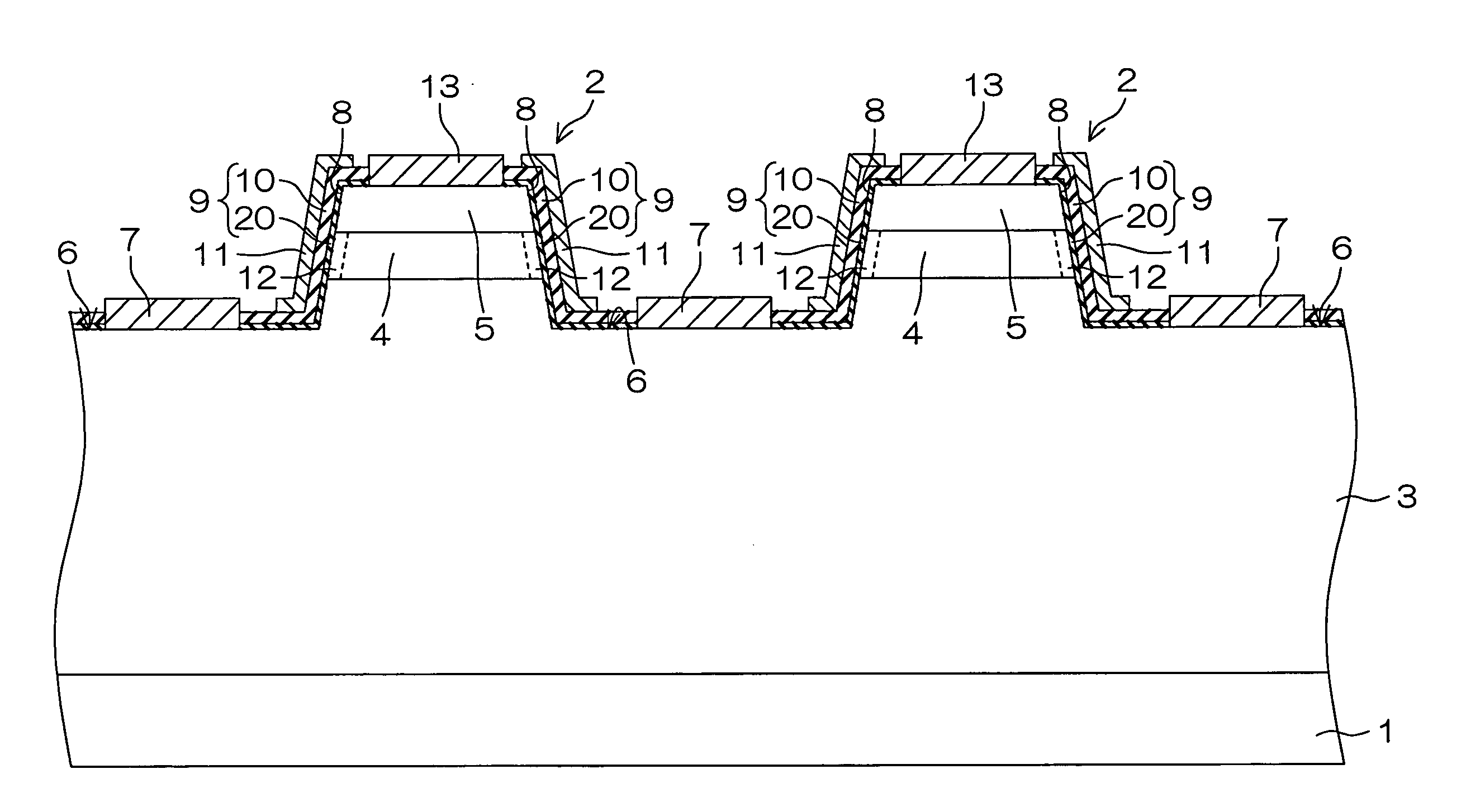
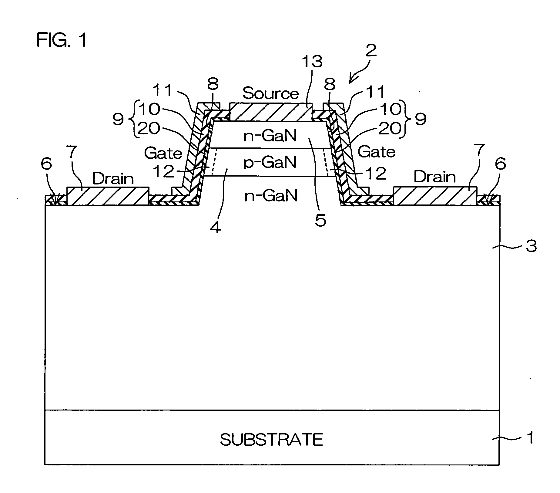
[0040]FIG. 1 is a schematic sectional view for illustrating the structure of a field-effect transistor according to the present invention.

[0041]This field-effect transistor (nitride semiconductor device) includes a substrate 1 and a nitride semiconductor laminated structure 2 made of a GaN compound semiconductor (group III nitride semiconductor) grown on the substrate 1.

[0042]For example, an insulating substrate such as a sapphire substrate or a conductive substrate such as a GaN substrate, a ZnO substrate, an Si substrate, a GaAs substrate or an SiC substrate can be applied to the substrate 1.

[0043]The nitride semiconductor laminated structure 2 includes an n-type GaN layer 3 (first layer), a p-type GaN layer 4 (second layer) and an n-type GaN layer 5 (third layer), which are laminated in this order. The nitride semiconductor laminated structure 2 is etched across the lamination interfaces from the n-type GaN layer 5 up to a depth exposing the n-type GaN layer 3, to have a trapezoi...

second embodiment

[0069]FIG. 3 is a schematic sectional view for illustrating the structure of a field-effect transistor according to the present invention.

[0070]This field-effect transistor (nitride semiconductor device) includes a substrate 15 and a p-type GaN layer 16, containing a p-type impurity, of a GaN compound semiconductor (group III nitride semiconductor) grown on the substrate 15.

[0071]For example, an insulating substrate such as a sapphire substrate or a conductive substrate such as a GaN substrate, a ZnO substrate, an Si substrate, a GaAs substrate or an SiC substrate can be applied to the substrate 15.

[0072]On the p-type GaN layer 16, a plurality of n-type regions 17 (second n-type region) and 18 (first n-type region) in the form of stripes in plan view are formed on the surface layer opposite to the substrate 15. The n-type regions 17 and 18 are alternately formed at prescribed intervals in a direction (referred to as “width direction” in this embodiment) orthogonal to the direction o...


PUM


Abstract

A method for producing a nitride semiconductor device according to the present invention includes the steps of: forming an insulating film containing oxygen on the surface of a group III nitride semiconductor; and placing the group III nitride semiconductor under a nitrogen atmosphere in advance of the step of forming the insulating film. A nitride semiconductor device according to the present invention includes a group III nitride semiconductor; and an insulating film containing oxygen formed on the surface of the group III nitride semiconductor, wherein the nitrogen concentration in a region provided with the insulating film is higher than the nitrogen concentration in a region not provided with the insulating film on the surface of the group III nitride semiconductor.

Description

BACKGROUND OF THE INVENTION[0001]1. Field of the Invention[0002]The present invention relates to a nitride semiconductor device using a Group III nitride semiconductor and a manufacturing method thereof.[0003]2. Description of Related Art[0004]Conventionally, a power device using a silicon semiconductor is used for a power amplifier circuit, a power supply circuit, a motor drive circuit, or the like. However, from theoretical limitations of the silicon semiconductor, high withstand voltage, low resistance, and high speed of the silicon device have nearly reached their limits, which leads to difficulties in satisfying market needs.[0005]Therefore, consideration has been given to the development of a nitride semiconductor device having characteristics such as high withstand voltage, high-temperature operation, a large current density, high-speed switching, low on-resistance, and the like.[0006]FIG. 5 is a schematic sectional view for illustrating the structure of a conventional field-...

Claims


Application Information

Patent Timeline
IPC IPC(8): H01L29/00H01L21/31
CPCH01L21/3185H01L21/8252H01L27/0605H01L29/7827H01L29/2003H01L29/66462H01L29/66666H01L29/045H01L21/0217
Inventor OTAKE, HIROTAKA
Owner ROHM CO LTD
Why Eureka
Try Eureka