Display device
- Summary
- Abstract
- Description
- Claims
- Application Information
AI Technical Summary
Benefits of technology
Problems solved by technology
Method used
Image
Examples
embodiment mode 1
[0072]In this embodiment mode, one mode of the present invention is described with reference to the drawings.
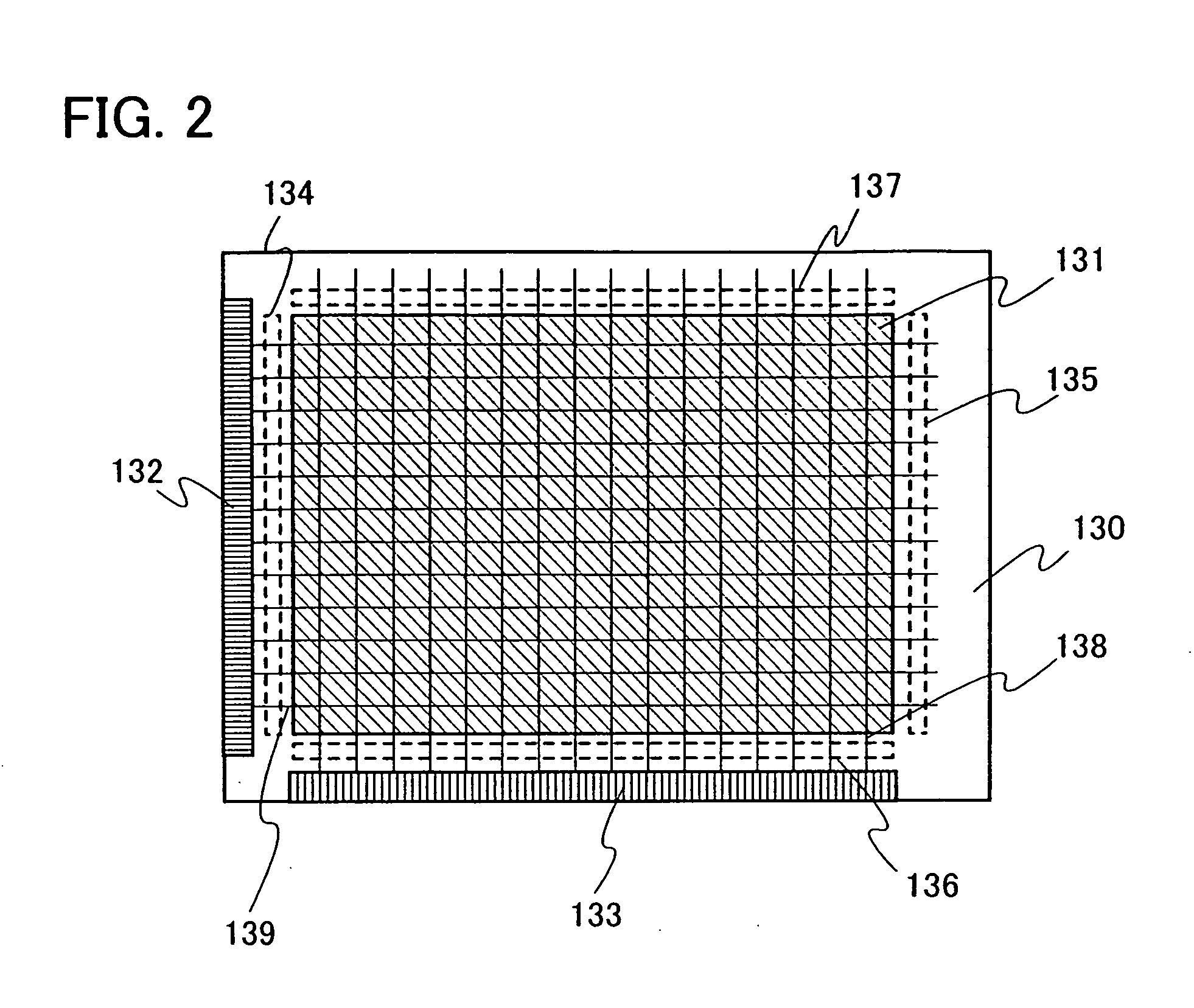
[0073]First, the structure of a semiconductor display device of the present invention is described with reference to FIG. 2. FIG. 2 is a top view of a substrate 130 over which a semiconductor display device is formed. A pixel portion 131 is formed over the substrate 130. In addition, an input terminal 132 and an input terminal 133 supply a signal and power for displaying images to a pixel circuit formed over the substrate 130.
[0074]Note that the present invention is not limited to the mode shown in FIG. 2. That is, one or both of a scan line driver circuit and a signal line driver circuit may be formed over the substrate 130.
[0075]The input terminal 132 on the scan line side and the input terminal 133 on the signal line side which are formed over the substrate 130 are connected to the pixel portion 131 by wirings extended vertically and horizontally. The wirings are connected...
embodiment mode 2
[0218]In this embodiment mode, a liquid crystal display device including a protection circuit using the thin film transistor shown in Embodiment Mode 1 is described.
[0219]First, a VA (vertical alignment)-mode liquid crystal display device is described. A VA-mode is a mode in which liquid crystal molecules are aligned vertically to a panel surface when voltage is not applied. In particular, in this embodiment mode, it is devised that a pixel is divided into several regions (subpixels) so that molecules are aligned in different directions. This is referred to as domain multiplication or multi-domain. In the following description, a multi-domain liquid crystal display device is described.
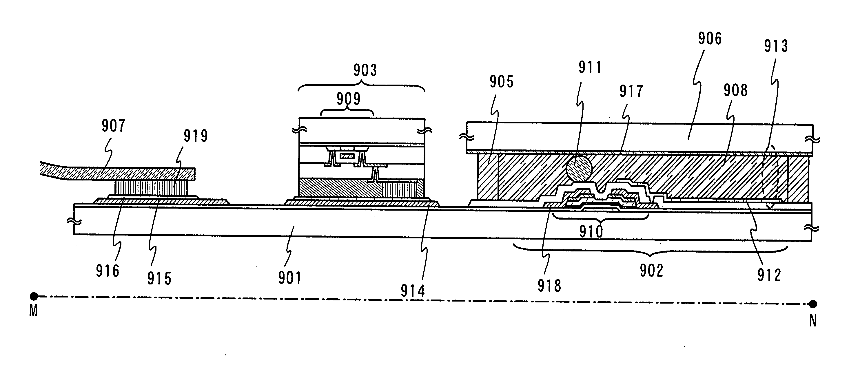
[0220]FIG. 9 is a plan view of a side of a substrate over which a pixel electrode is formed. FIG. 8 shows a cross-sectional structure taken along the line A-B in FIG. 9. In addition, FIG. 10 is a plan view of a side of a substrate on which a counter electrode is formed. Hereinafter, description is made...
embodiment mode 3
[0264]The present invention can be applied not only to a liquid crystal display device but also a light-emitting device. In this embodiment mode, a manufacturing process and the like of light-emitting devices are described with reference to FIGS. 22A and 22B and FIGS. 23A to 23C. A light-emitting element utilizing electroluminescence is used for a light-emitting device. Light-emitting elements utilizing electroluminescence are classified according to whether a light-emitting material is an organic compound or an inorganic compound. In general, the former is referred to as organic EL elements and the latter as inorganic EL elements.
[0265]In an organic EL element, when voltage is applied to a light-emitting element, electrons and holes are injected from a pair of electrodes into a layer containing a light-emitting organic compound, and current flows. Then, recombination of these carriers (the electrons and holes) makes the light-emitting organic compound to form an excited state and t...
PUM
 Abstract
Description
Claims
Application Information
 - R&D
- Intellectual Property
- Life Sciences
- Materials
- Tech Scout
- Unparalleled Data Quality
- Higher Quality Content
- 60% Fewer Hallucinations
Browse by: Latest US Patents, China's latest patents, Technical Efficacy Thesaurus, Application Domain, Technology Topic, Popular Technical Reports.
© 2025 PatSnap. All rights reserved.Legal|Privacy policy|Modern Slavery Act Transparency Statement|Sitemap|About US| Contact US: help@patsnap.com


