
Nitride semiconductor light emitting device and fabrication method thereof

a light emitting device and semiconductor technology, applied in semiconductor/solid-state device manufacturing, semiconductor devices, semiconductor devices, etc., can solve the problems of increasing the leakage current of the device, gan based light emitting device has a bad static electricity characteristic, and gan thin film is prone to crystal defects. , to achieve the effect of reducing the leakage current, preventing the damage of the light emitting device, and increasing the resistance in the region

Active Publication Date: 2009-01-15
SAMSUNG ELECTRONICS CO LTD
View PDF8 Cites 133 Cited by
  • Summary
  • Abstract
  • Description
  • Claims
  • Application Information

AI Technical Summary

Benefits of technology

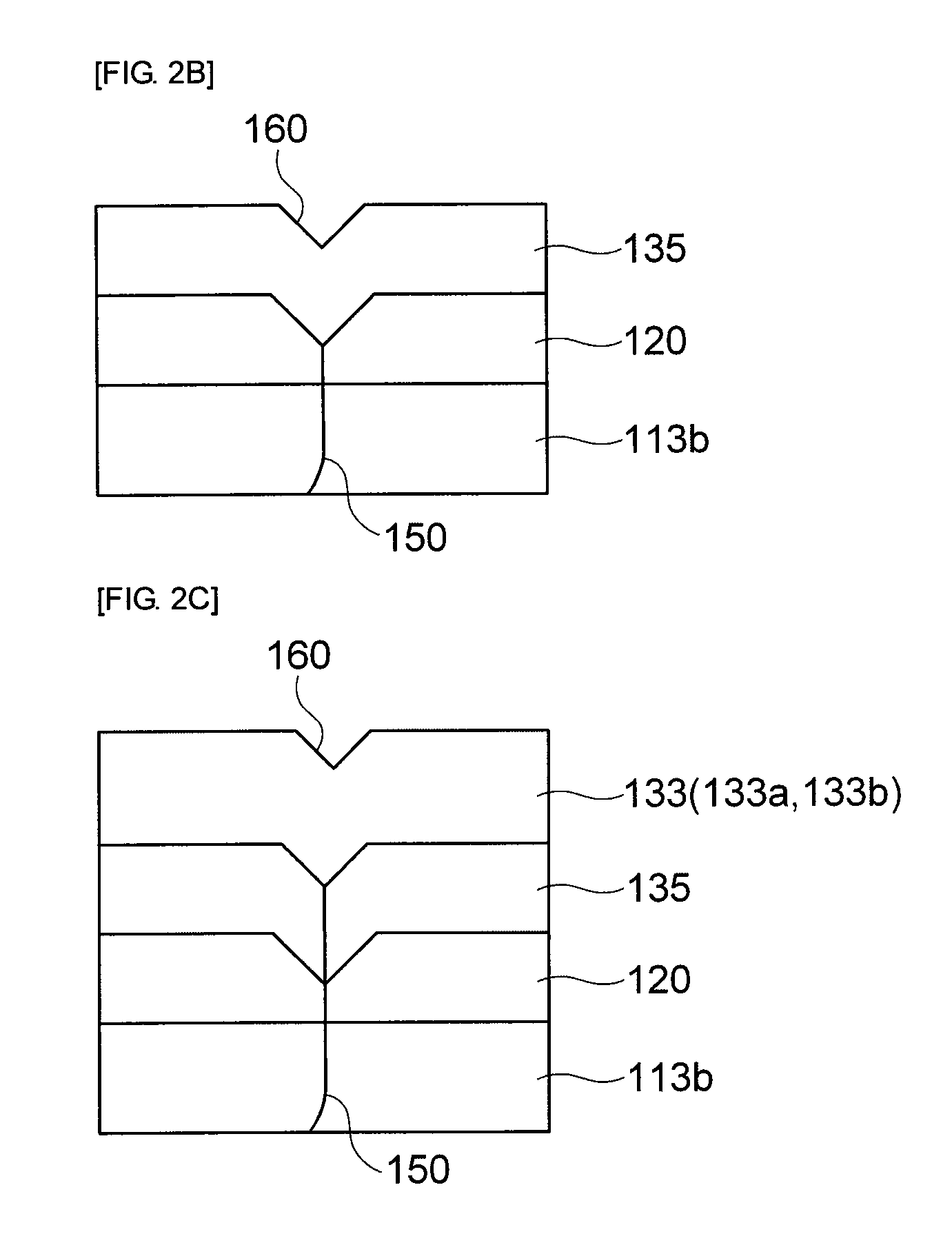
The present invention provides a nitride semiconductor light emitting device and a fabrication method thereof that can improve ESD effect by reducing leakage currents inversely using crystal defects (threading dislocations) that were the reason for conventional leakage currents. The device includes a substrate, an n-type semiconductor layer, an active layer, a p-type semiconductor layer, a transparent electrode, and a bonding electrode. The device also includes a V-shaped distortion layer formed with reference to threading dislocations. The invention provides a nitride semiconductor light emitting device that can reduce leakage currents and improve ESD effect.

Problems solved by technology

Generally, it has been known that a GaN based light emitting device has a bad static electricity characteristic in comparison with other compound light emitting devices.
This reason is that a lot of crystal defects are formed in a GaN thin film due to a great lattice mismatch (16%) between a substrate and a thin film to be grown since the GaN light emitting device is formed on a sapphire substrate having a great lattice mismatch.
This crystal defect increases a leakage current of device and an active layer of the light emitting device having a lot of crystal defects is broken by a strong field when an external static electricity is applied.
The static electricity broken characteristic of the light emitting device is a very important issue related to the application range of the GaN based light emitting device.
Particularly, since the GaN light emitting device generally employs a sapphire substrate as an insulator, the ESD characteristic is further deteriorated by increasing a concentration phenomenon of currents around an N-electrode during a practical device operation as the N-electrode and a P-electrode are formed at the same plane on the structure of the device.
However, since such methods cause complicatedness to be assembled by purchasing an additional Zenor diode or performing a Schottky junction and increase the manufacturing cost of the device, they are not preferable in point of cost or yield.

Method used


Image

  • Nitride semiconductor light emitting device and fabrication method thereof
  • Nitride semiconductor light emitting device and fabrication method thereof
  • Nitride semiconductor light emitting device and fabrication method thereof

Examples


Embodiment Construction

[0054]Hereinafter, an apparatus for forming a nitride semiconductor light emitting device and a method for forming a fabrication method thereof in accordance with the present invention will be described in detail with reference to the accompanying drawings.

[0055]FIG. 1 is a cross sectional view showing a structure of a nitride semiconductor light emitting device (LED) in accordance with the present invention.

[0056]As shown in FIG. 1, a nitride semiconductor light emitting device 100 in accordance with the present invention includes a substrate 110, a buffer layer 111 formed on the substrate 100, a light emitting structure made of n-type nitride semiconductor layers 113 and 115, an active layer 120 and p-type nitride semiconductor layers 135 and 133 sequentially stacked on the buffer layer 111, and a V-shaped distortion structure layer 160 formed with reference to a penetration defect penetrating into at least one portion of the light emitting structure. At this time, an un-doped GaN...


PUM


Abstract

The present invention relates to a GaN based nitride based light emitting device improved in Electrostatic Discharge (ESD) tolerance (withstanding property) and a method for fabricating the same including a substrate and a V-shaped distortion structure made of an n-type nitride semiconductor layer, an active layer and a p-type nitride semiconductor layer on the substrate and formed with reference to the n-type nitride semiconductor layer.

Description

CROSS-REFERENCE TO RELATED APPLICATIONS[0001]This application claims the benefit of Korean Patent Application No. 10-2007-0070107 filed with the Korea Intellectual Property Office on Jul. 12, 2007, the disclosure of which is incorporated herein by reference.BACKGROUND OF THE INVENTION[0002]1. Field of the Invention[0003]The present invention relates to a nitride semiconductor light emitting device; and, more particularly, to a nitride semiconductor light emitting device capable of improving an ESD (Electrostatic Discharge) tolerance (withstand voltage characteristic) of a GaN based nitride light emitting device and a method for manufacturing the same.[0004]2. Description of the Related Art[0005]Generally, it has been known that a GaN based light emitting device has a bad static electricity characteristic in comparison with other compound light emitting devices. This reason is that a lot of crystal defects are formed in a GaN thin film due to a great lattice mismatch (16%) between a ...

Claims


Application Information

Patent Timeline
Patent Type & Authority Applications(United States)
IPC IPC(8): H01L33/00H01L33/22H01L33/24H01L33/32
CPCH01L33/22H01L33/0075H01L33/32H01L33/24
Inventor KANG, SANG WONKIM, YONG CHUNCHO, DONG HYUNOH, JEONG TAKKIM, DONG JOON
Owner SAMSUNG ELECTRONICS CO LTD
Learn More