Light-emitting element, light-emitting device, electronic device, and method for fabricating light-emitting element
a technology of light-emitting elements and electronic devices, which is applied in the manufacture of electrode systems, electric discharge tubes/lamps, and discharge tubes luminescnet screens, etc., can solve the problems of short life of elements, and easy deterioration of light-emitting elements, etc., to achieve long life, not easy to deteriorate, and long life
- Summary
- Abstract
- Description
- Claims
- Application Information
AI Technical Summary
Benefits of technology
Problems solved by technology
Method used
Image
Examples
embodiment mode 1
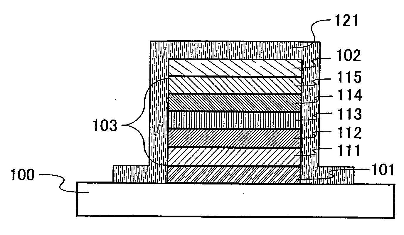
[0043]In this embodiment mode, a light-emitting element in which a first sealing layer is provided is described.
[0044]The light-emitting element of the present invention has a plurality of layers between a pair of electrodes. The plurality of layers is formed of a stack of layers formed of a substance having a high carrier-injecting property and a substance having a high carrier-transporting property. These layers are stacked so that a light-emitting region is formed in a region away from the electrodes, that is, so that recombination of carriers is performed in an area away from the electrodes.
[0045]In FIG. 1, a substrate 100 is used as a support of the light-emitting element. For the substrate 100, glass, plastic, or the like can be used. It is to be noted that any material other than these may be used as long as it functions as a support of the light-emitting element in a fabrication process of the light-emitting element. Alternatively, a flexible substrate may be used as the sub...
embodiment mode 2
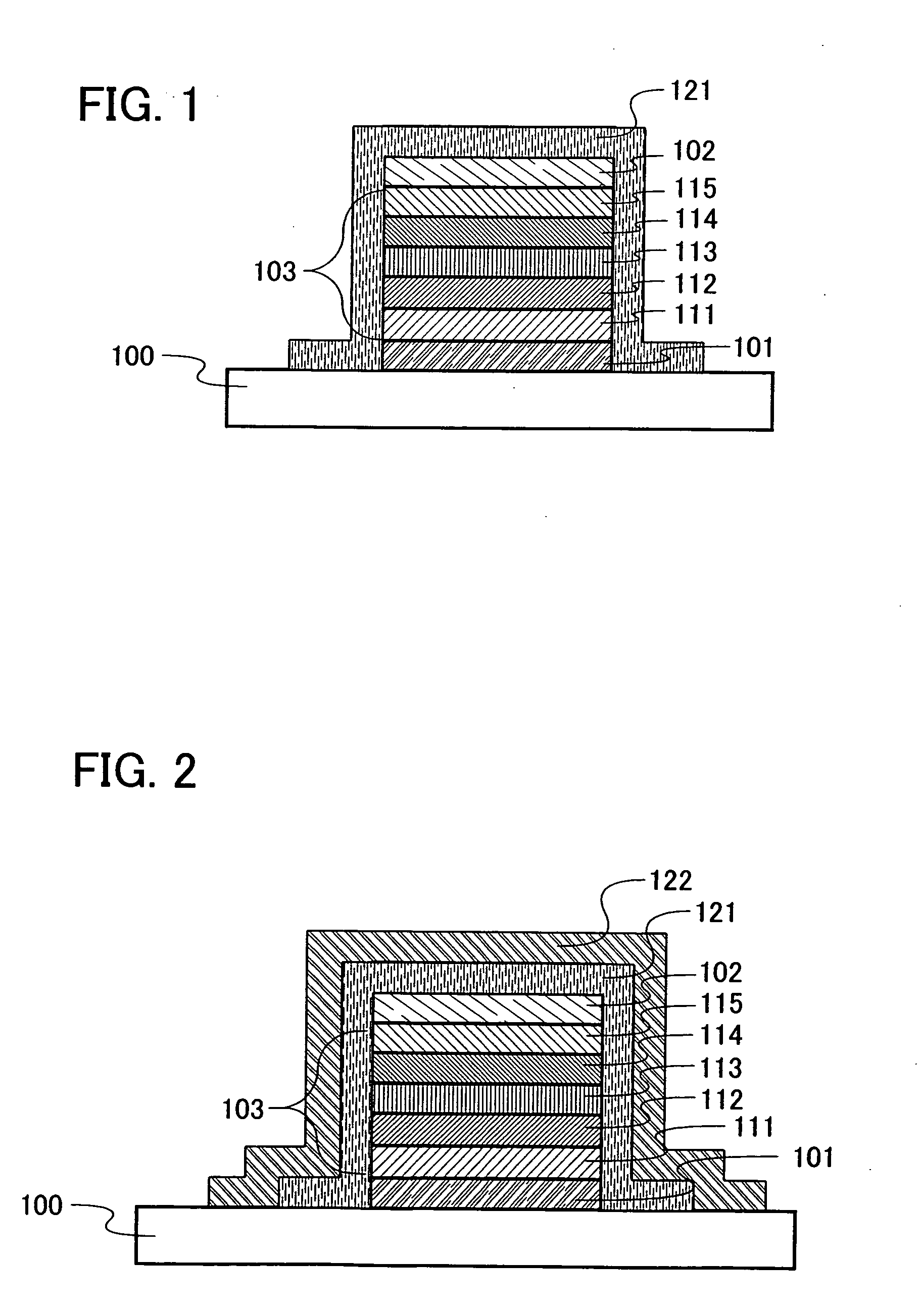
[0090]In this embodiment mode, a light-emitting element in which a second sealing layer is provided is described using FIG. 2.
[0091]In this embodiment mode, a light-emitting element includes the first electrode 101, the second electrode 102, the EL layer 103 provided between the first electrode 101 and the second electrode 102, the first sealing layer 121 formed over the second electrode, and a second sealing layer 122 formed over the first sealing layer 121. That is, the light-emitting element of this embodiment mode includes a second sealing layer that is formed so as to cover the light-emitting element described in Embodiment Mode 1.
[0092]The second sealing layer 122 is a passivation film formed of an inorganic compound and has low moisture / oxygen permeability and superior mechanical strength. Specifically, silicon nitride, silicon nitride oxide, silicon oxide, aluminum oxide, aluminum nitride, aluminum nitride oxide, diamond-like carbon (DLC), or the like can be used. Alternativ...
embodiment mode 3
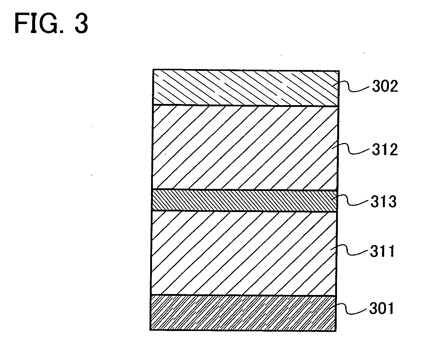
[0099]In this embodiment mode, a mode of a light-emitting element in which a plurality of light-emitting units according to the present invention is stacked (hereinafter, referred to as a stacked-type element) is described with reference to FIG. 3. The light-emitting element is a stacked-type light-emitting element including a plurality of light-emitting units between a first electrode and a second electrode. Each light-emitting unit can be made to have an EL layer that is similar to that described in Embodiment Mode 1. That is, the light-emitting element described in Embodiment Mode 1 is a light-emitting element including one light-emitting unit. The light-emitting unit includes at least a light-emitting layer, and there is no particular limitation on a structure of a stack of other layers. In this embodiment mode, a light-emitting element including a plurality of light-emitting units is described.
[0100]In FIG. 3, a first light-emitting unit 311, a charge generation layer 313, and ...
PUM
| Property | Measurement | Unit |
|---|---|---|
| Thickness | aaaaa | aaaaa |
| Thickness | aaaaa | aaaaa |
| Concentration | aaaaa | aaaaa |
Abstract
Description
Claims
Application Information
 - R&D
- Intellectual Property
- Life Sciences
- Materials
- Tech Scout
- Unparalleled Data Quality
- Higher Quality Content
- 60% Fewer Hallucinations
Browse by: Latest US Patents, China's latest patents, Technical Efficacy Thesaurus, Application Domain, Technology Topic, Popular Technical Reports.
© 2025 PatSnap. All rights reserved.Legal|Privacy policy|Modern Slavery Act Transparency Statement|Sitemap|About US| Contact US: help@patsnap.com


