
Plasma processing apparatus and method

Inactive Publication Date: 2008-12-25
SAMSUNG ELECTRONICS CO LTD
View PDF3 Cites 79 Cited by
  • Summary
  • Abstract
  • Description
  • Claims
  • Application Information

AI Technical Summary

Benefits of technology

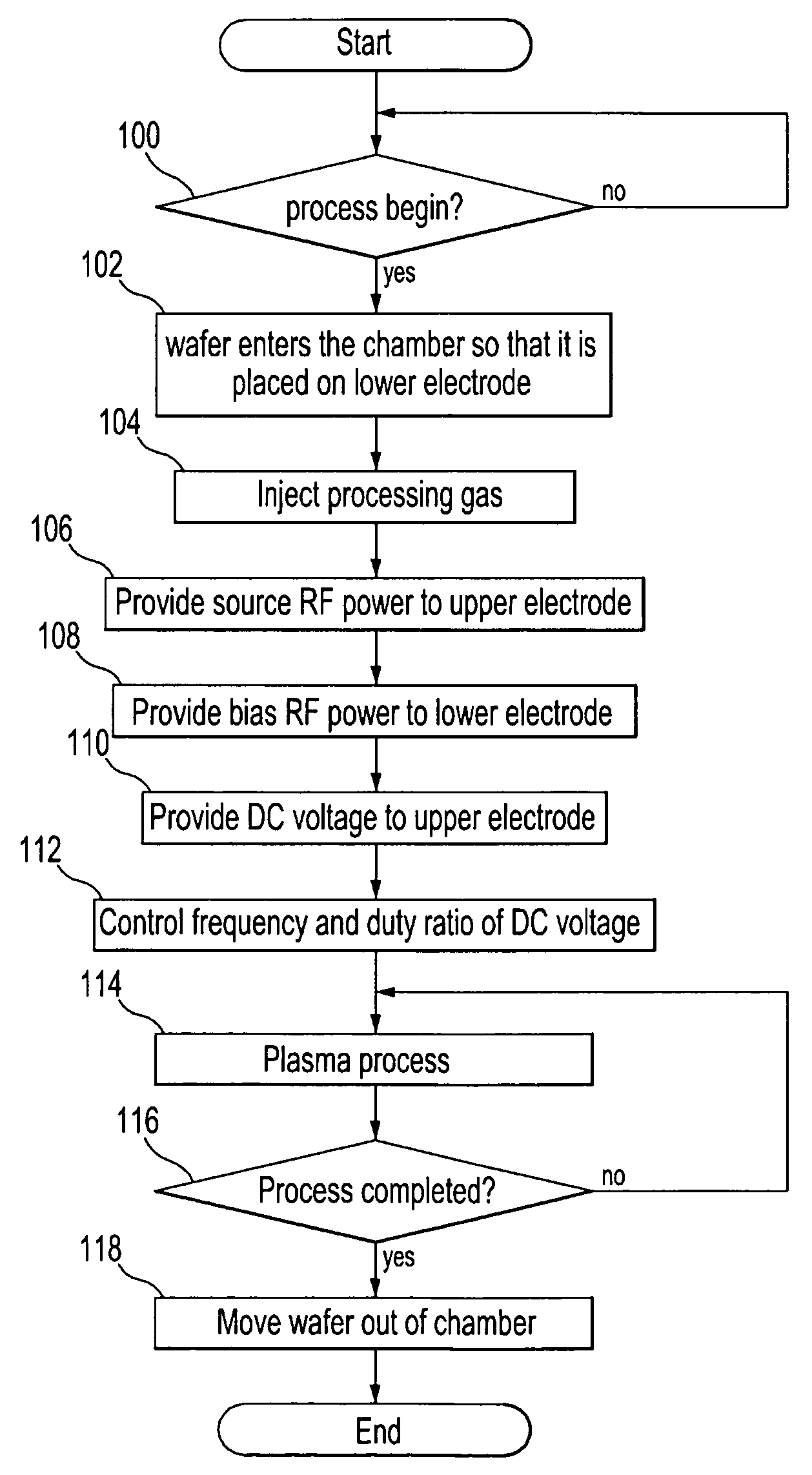
[0014]Therefore, it is an aspect of the invention to provide a plasma processing apparatus and method for maximizing the plasma electron density in a plasma process in which the semiconductor substrate is processed using the plasma, so that it can increase the semiconductor processing rate.
[0015]It is another aspect of the invention to provide a plasma processing apparatus and method for applying a DC voltage to an electrode receiving a source RF power so as to confine electrons of the plasma, thereby maximizing the plasma electron density.
[0016]It is yet another aspect of the invention to provide a plasma processing apparatus and method for applying a pulse-format DC voltage, resulting in the prevention of the danger of etching the electrode receiving the source RF power. The etching of the electrode is caused by the electrons excessively accumulated in the plasma.

Problems solved by technology

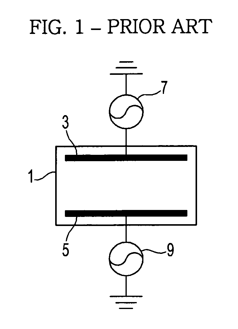
However, the devices of the high frequency unavoidably encounter the problem of the processing etching uniformity due to sine waves generated from the electrodes 3 and 5.
However, electrons contained in the plasma of the RF power-supply system of the conventional plasma processing apparatus are emitted to the electrode (reference number 3 or 5) receiving the source RF power, so that the high plasma electron density cannot be maintained.
However, the RF power-supply system cannot certainly confine low-temperature electrodes of the plasma according to the variation of a semiconductor fabrication process.
The etching of the electrode is caused by the electrons excessively accumulated in the plasma.

Method used


Image

  • Plasma processing apparatus and method
  • Plasma processing apparatus and method
  • Plasma processing apparatus and method

Examples


Embodiment Construction

[0035]Reference will now be made in detail to the embodiments of the present invention, examples of which are illustrated in the accompanying drawings, wherein like reference numerals refer to like elements throughout. The embodiments are described below to explain the present invention by referring to the figures.

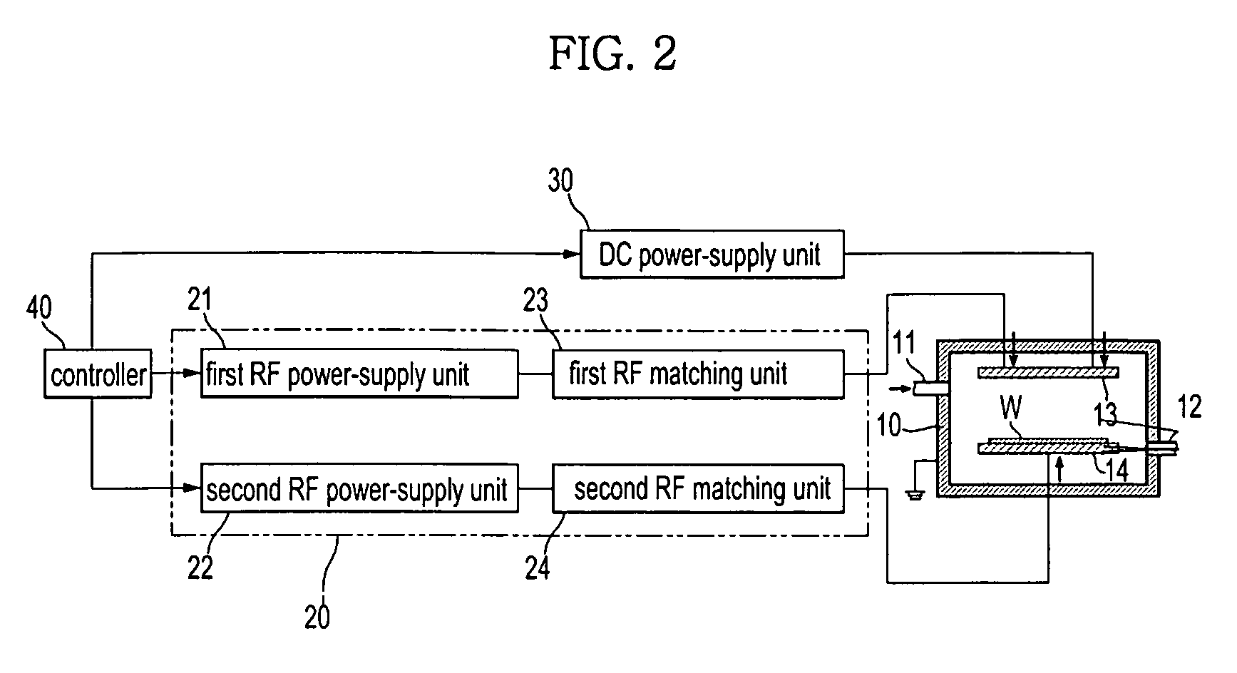
[0036]FIG. 2 is a block diagram illustrating a RF power-supply system according to the present invention.

[0037]Referring to FIG. 2, the plasma processing apparatus according to the present invention includes a chamber 10, a RF power-supply unit 20, a DC power-supply unit 30, and a controller 40.

[0038]The chamber 10 is a vacuum-status processing chamber in which the semiconductor fabrication process based on the plasma is conducted, and acts as a reactor for processing the etching process such as a wafer (W) used as the semiconductor substrate. In the chamber 10, a gas inlet 11 and a gas outlet 12 are formed, the gas supplied from the gas inlet 11 is excited into the plasma...


PUM

PropertyMeasurementUnit
Fractionaaaaaaaaaa
Fractionaaaaaaaaaa
Electric potential / voltageaaaaaaaaaa

Abstract

The plasma processing apparatus for processing a semiconductor substrate using plasma and a method thereof can maintain a steady state simultaneously while maximizing a plasma electron density. The plasma processing apparatus includes: a chamber which generates plasma to process a semiconductor substrate; upper and lower electrodes arranged in the chamber; a DC power-supply unit which applies a DC voltage to either one of the upper and lower electrodes; and a controller which adjusts a power ratio of the DC voltage applied from the DC power-supply unit to either one of the upper and lower electrodes. As a result, the apparatus certainly confines electrons, so that the electrodes are not emitted from the plasma, resulting in a maximized plasma electron density.

Description

CROSS-REFERENCE TO RELATED APPLICATIONS[0001]This application claims the benefit of Korean Patent Application No. 2007-0059805, filed on Jun. 19, 2007 in the Korean Intellectual Property Office, the disclosure of which is incorporated herein by reference.BACKGROUND[0002]1. Field[0003]The present invention relates to a method for manufacturing a semiconductor using plasma, and more particularly to a plasma processing apparatus and method for maximizing a plasma electron density to increase a semicircular fabrication speed.[0004]2. Description of the Related Art[0005]Generally, the semiconductor fabrication process has widely used a plasma processing apparatus for etching or depositing a semiconductor substrate using the plasma. A variety of plasma processing apparatuses have been widely used for the plasma processing apparatus. A representative example of the plasma processing apparatus is a Capacitive Coupled Plasma (CCP) processing apparatus.[0006]The CCP processing apparatus arran...

Claims


Application Information

Patent Timeline
IPC IPC(8): C23C14/32C23F1/00
CPCC23C16/5096H01J37/32009H01J37/32027H01J37/32091H01J37/32532
Inventor SON, GIL SUSUNG, DOUG YONGKWON, TAE YONGLIM, KYUNG CHUN
Owner SAMSUNG ELECTRONICS CO LTD
Learn More