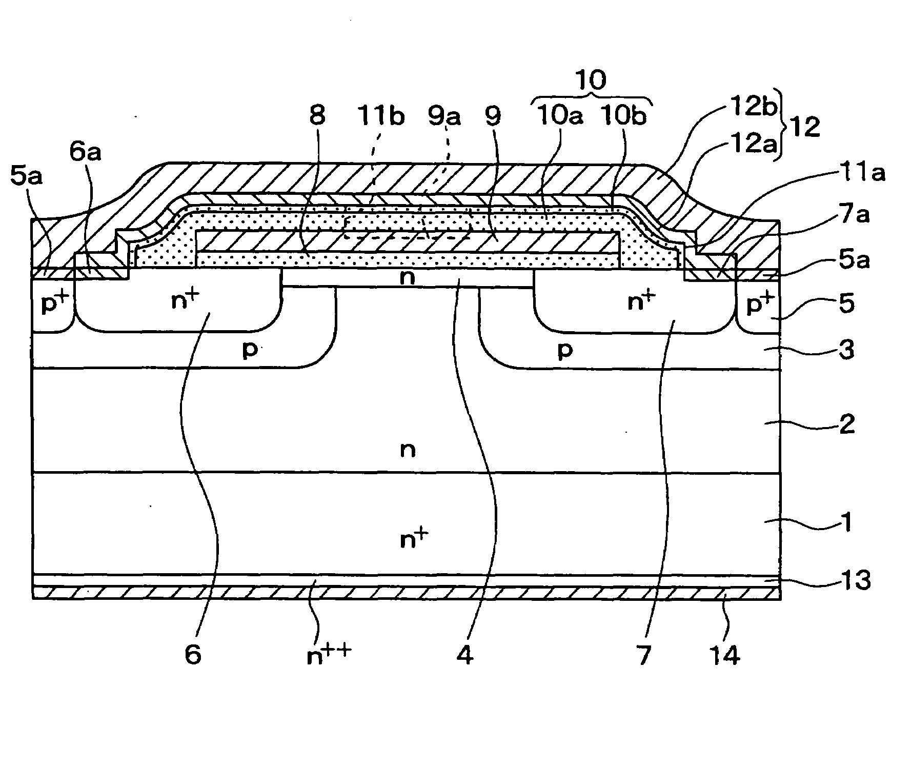
[0008]According to a first aspect of the present disclosure, a SiC
semiconductor device includes: a substrate made of SiC and having first and second sides; a drift layer made of SiC, having a N conductive type, and disposed on the first side of the substrate; a base region having a P conductive type, and disposed in a surface portion of the drift layer; a source region made of SiC, having the N conductive type, disposed in the base region, wherein an
impurity concentration of the source region is higher than the drift layer; a channel layer made of SiC, having the N conductive type, and disposed on the base region and the drift layer, wherein the channel layer connects the drift layer and the source region; a
gate oxide film disposed on the channel layer and the source region; a gate electrode disposed on the gate
oxide film; an interlayer insulation film disposed on the gate electrode, wherein the interlayer insulation film includes a contact hole, which connects to the base region and the source region; a source electrode disposed in the contact hole of the interlayer insulation film so that the source electrode is electrically coupled with the base region and the source region; and a drain electrode disposed on the second side of the substrate. The channel layer provides a channel, which is controllable with a
voltage applied to the gate electrode. The channel provides a current flowing between the source electrode and the drain electrode through the source region, the channel and the drift layer. The source electrode includes a lower wiring electrode and an upper wiring electrode. The lower wiring electrode is made of material including a Ni component for providing
ohmic contact with respect to a N conductive type semiconductor. The lower wiring electrode is disposed on the interlayer insulation film. The lower wiring electrode is electrically coupled with the source region. The upper wiring electrode is made of material for providing
ohmic contact with respect to a P conductive type semiconductor. The upper wiring electrode is disposed on the lower wiring electrode. The upper wiring electrode is electrically coupled with the base region. The interlayer insulation film further includes a BPSG insulation film and a
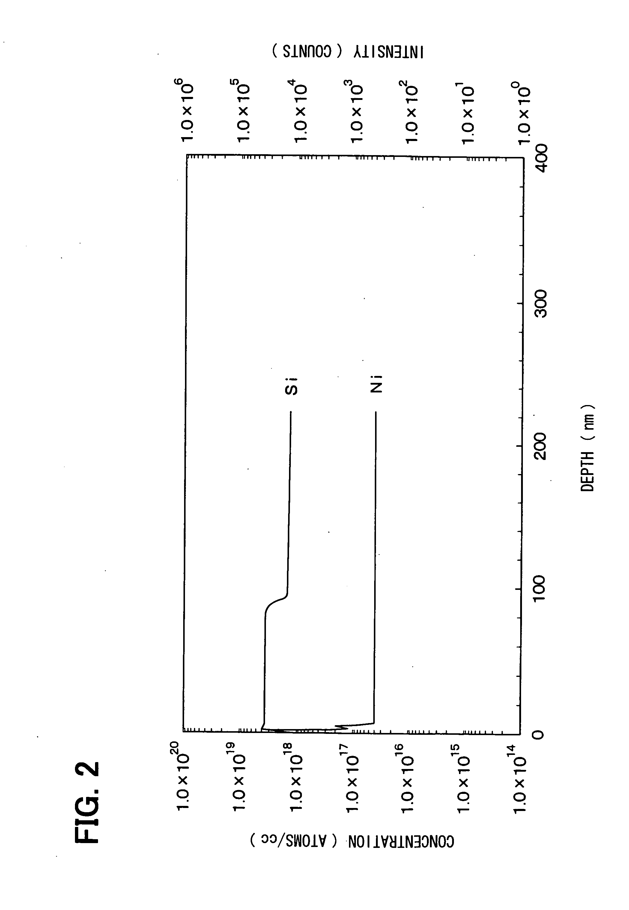
barrier layer. The BPSG insulation film is disposed on the gate electrode. The barrier layer is disposed on the BPSG insulation film and provides a sidewall of the contact hole of the interlayer insulation film. The barrier layer prevents the Ni component in the lower wiring electrode from being diffused into the BPSG insulation film.
[0009]In the above device, the BPSG insulation film does not contact the lower wiring electrode in the source electrode. Therefore, the Ni component in the lower wiring electrode is prevented from being diffused into the BPSG insulation film.
[0010]According to a second aspect of the present disclosure, a SiC semiconductor device includes: a substrate made of SiC and having first and second sides; a drift layer made of SiC, having a N conductive type, and disposed on the first side of the substrate; a base region having a P conductive type, and disposed in a surface portion of the drift layer; a source region made of SiC, having the N conductive type, disposed in the base region, wherein an
impurity concentration of the source region is higher than the drift layer; a gate
oxide film disposed on the drift layer, the base region and the source region; a gate electrode disposed on the gate
oxide film; an interlayer insulation film disposed on the gate electrode, wherein the interlayer insulation film includes a contact hole, which connects to the base region and the source region; a source electrode disposed in the contact hole of the interlayer insulation film so that the source electrode is electrically coupled with the base region and the source region; and a drain electrode disposed on the second side of the substrate. A part of the base region facing the gate electrode through the gate insulation film provides a channel, which is controllable with a
voltage applied to the gate electrode. The channel provides a current flowing between the source electrode and the drain electrode through the source region, the channel and the drift layer. The source electrode includes a lower wiring electrode and an upper wiring electrode. The lower wiring electrode is made of material including a Ni component for providing
ohmic contact with respect to a N conductive type semiconductor. The lower wiring electrode is disposed on the interlayer insulation film. The lower wiring electrode is electrically coupled with the source region. The upper wiring electrode is disposed on the lower wiring electrode. The upper wiring electrode is electrically coupled with the base region. The interlayer insulation film further includes a BPSG insulation film and a barrier layer. The BPSG insulation film is disposed on the gate electrode. The barrier layer is disposed on the BPSG insulation film and provides a sidewall of the contact hole of the interlayer insulation film. The barrier layer prevents the Ni component in the lower wiring electrode from being diffused into the BPSG insulation film.
[0011]In the above device, the BPSG insulation film does not contact the lower wiring electrode in the source electrode. Therefore, the Ni component in the lower wiring electrode is prevented from being diffused into the BPSG insulation film.
[0013]In the above method, the BPSG insulation film does not contact the lower wiring electrode in the source electrode. Therefore, the Ni component in the lower wiring electrode is prevented from being diffused into the BPSG insulation film.
[0015]In the above method, the BPSG insulation film does not contact the lower wiring electrode in the source electrode. Therefore, the Ni component in the lower wiring electrode is prevented from being diffused into the BPSG insulation film.
