Eureka AIR delivers breakthrough ideas for toughest innovation challenges, trusted by R&D personnel around the world.

Images with high speed digital frame transfer and frame processing

a digital frame transfer and image sensor technology, applied in the field of imagers with high-speed digital frame transfer, can solve the problems of high frame rate, high frame rate, and high shutter speed, and achieve the effect of reducing the cost of image processing, high frame rate, and high frame ra

Active Publication Date: 2008-12-18
APTINA IMAGING CORP
View PDF35 Cites 80 Cited by
  • Summary
  • Abstract
  • Description
  • Claims
  • Application Information

AI Technical Summary

Problems solved by technology

It can range in complexity from a simple spring-loaded pinhole punched in a dark plate to the complicated multiple-blade single-lens reflex (SLR) structure.
These shutters are not fast enough, or reliable enough, to operate at high frame rates.
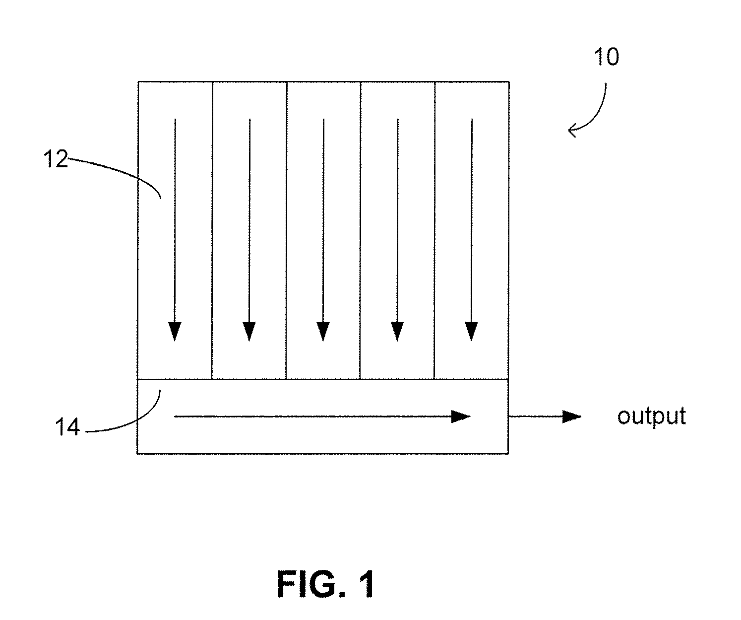
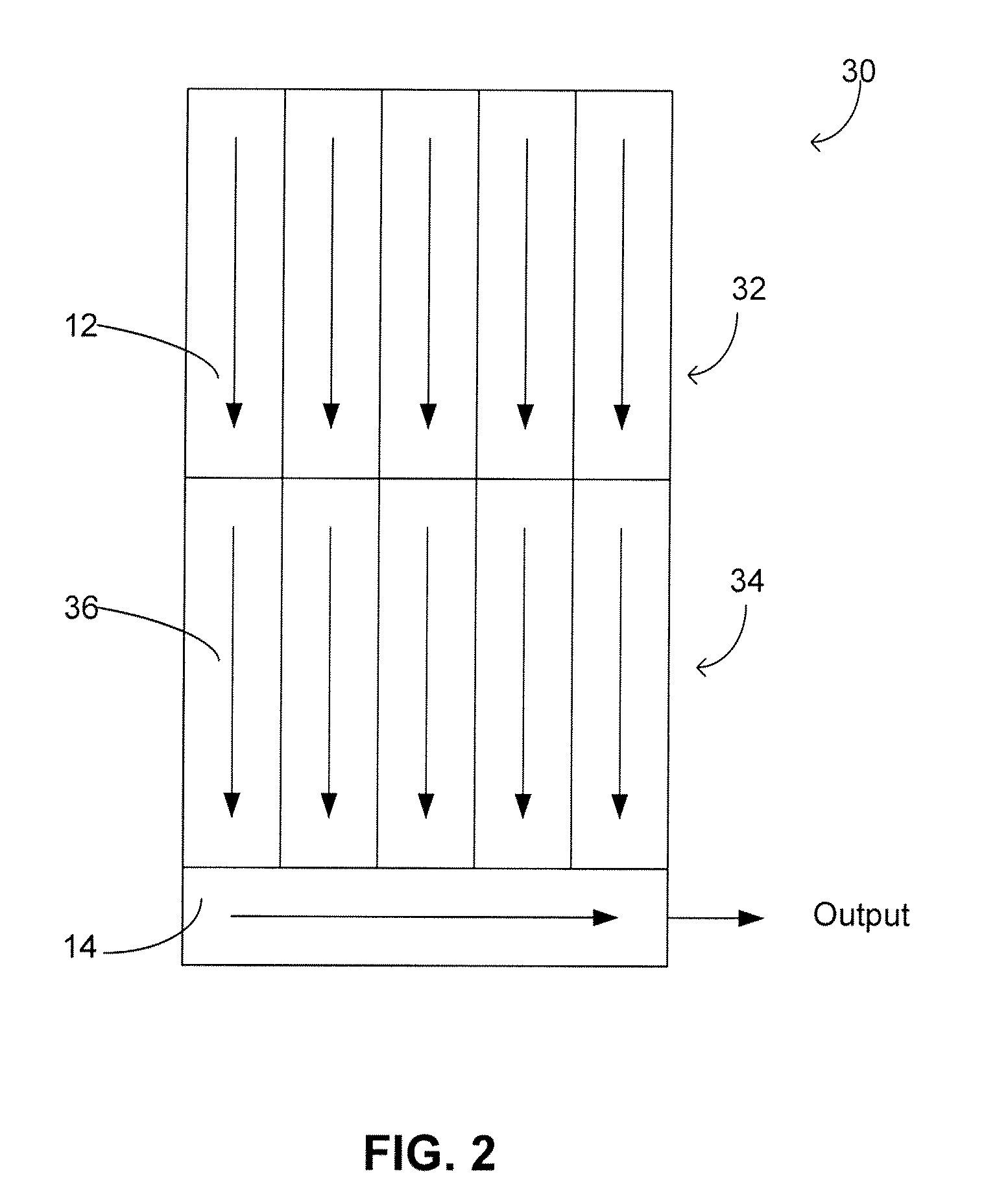
In addition, this type of image sensor 30 is costly because the area of the sensor 30 is roughly doubled.
Moreover, the image may also be corrupted by dark current while it is being stored.
However, it is burdensome and extremely difficult (if not impossible) to completely mask the vertical register 52 structures from light.
As can be appreciated, however, the frame interline transfer CCD image sensor 70 is relatively expensive and is generally used only in commercial broadcast cameras.
Because it is difficult to keep stray light from reaching the floating diffusion region FD, the global shutter method of operating a CMOS image sensor also suffers from smear.
As is known in the art, the CMOS image sensor also suffers from kT / C noise because correlated double sampling is not performed when using the global shutter mode of operation.
If there is any motion in the scene, however, the varying integration interval causes motion artifacts to appear.

Method used


Image

  • Images with high speed digital frame transfer and frame processing
  • Images with high speed digital frame transfer and frame processing
  • Images with high speed digital frame transfer and frame processing

Examples


Embodiment Construction

[0032]In the following detailed description, reference is made to the accompanying drawings which form a part hereof, and in which is shown by way of illustration specific embodiments that may be practiced. These embodiments are described in sufficient detail to enable those of ordinary skill in the art to make and use them, and it is to be understood that structural, logical, or procedural changes may be made to the specific embodiments disclosed.

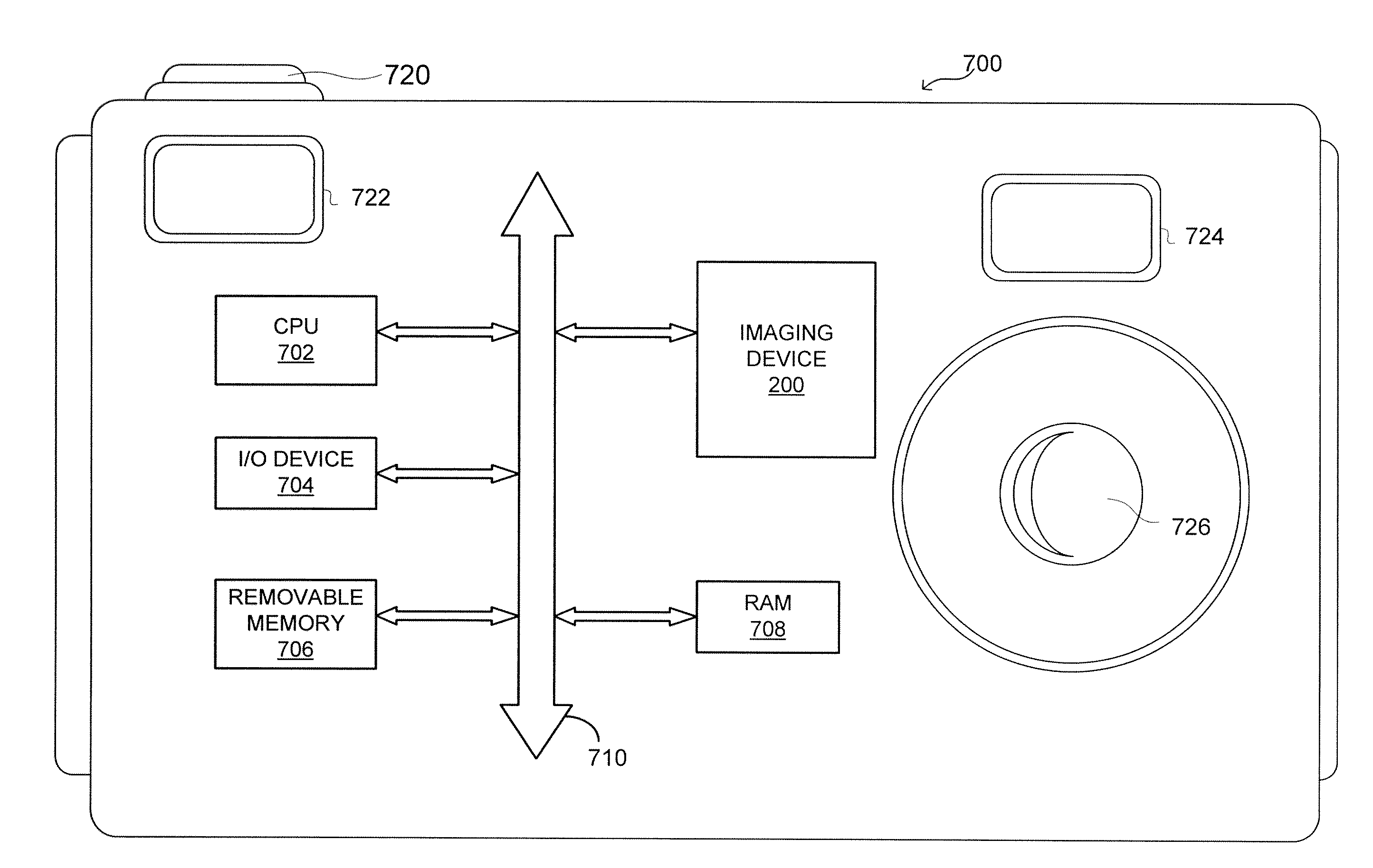
[0033]Embodiments disclosed herein provide a CMOS image sensor that captures images substantially free of smear and kT / C noise and in which motion artifacts are substantially minimized. The embodiments are analogous to frame transfer techniques except that they use a rolling shutter operational method and a digital memory integrated with the image sensor (either in the same chip or in the same package). The embodiments may be referred to as implementing a digital frame transfer and / or a digital frame transfer imager.

[0034]The embodiments d...


PUM


Abstract

A digital frame transfer imager having an image sensor and frame memory in the same chip. The image sensor has an integrated memory controller for controlling transfers of data between the sensor and the memory array. The imager utilizes a rolling shutter and multiple groups of analog-to-digital processing circuitry to readout data from the sensor and to output digital images substantially free from image smear, kT / C noise and other unwanted image artifacts.

Description

FIELD OF THE INVENTION[0001]Embodiments of the invention relate to semiconductor imaging devices and more particularly to imagers with high speed digital frame transfer.BACKGROUND OF THE INVENTION[0002]The exposure of an image detector such as an image sensor must be controlled to prevent overexposure, which causes clipping, and underexposure which results in excessive noise. Exposure control is generally accomplished by a shutter that blocks light when it is closed, and allows light to pass when it is open. Aperture control and neutral density filters can be used to reduce the intensity of light, and to allow the image detector to build up its exposure more gradually. However, virtually all cameras implement shutters.[0003]In film cameras, the shutter is a mechanical mechanism. It can range in complexity from a simple spring-loaded pinhole punched in a dark plate to the complicated multiple-blade single-lens reflex (SLR) structure. These shutters are not fast enough, or reliable en...

Claims


Application Information

Patent Timeline
IPC IPC(8): H04N5/76H04N5/335H04N5/347H04N5/355H04N5/357H04N5/3745H04N5/378
CPCH04N5/235H04N5/347H04N5/3532H04N5/3742H04N5/3745H04N5/378H04N23/70H04N25/531H04N25/46H04N25/767H04N25/77H04N25/75H04N3/1556H04N3/1562H04N3/1575H04N25/63H04N25/41
Inventor SMITH, SCOTTBAER, RICHARD L.SAVIDGE, LAURA
Owner APTINA IMAGING CORP
Why Eureka
Eureka Blog
Learn More