
Method of fabricating polycrystalline silicon layer, TFT fabricated using the same, method of fabricating TFT, and organic light emitting diode display device having the same

a technology of polycrystalline silicon and thin film transistor, which is applied in the direction of transistors, solid-state devices, thermoelectric devices, etc., can solve the problems of long processing time and risk of substrate transformation, poor interfacial characteristics between a semiconductor layer and a gate insulating layer, and high cost of laser equipment. achieve the effect of reducing leakage curren

Inactive Publication Date: 2008-12-04
SAMSUNG MOBILE DISPLAY CO LTD
View PDF51 Cites 40 Cited by
  • Summary
  • Abstract
  • Description
  • Claims
  • Application Information

AI Technical Summary

Benefits of technology

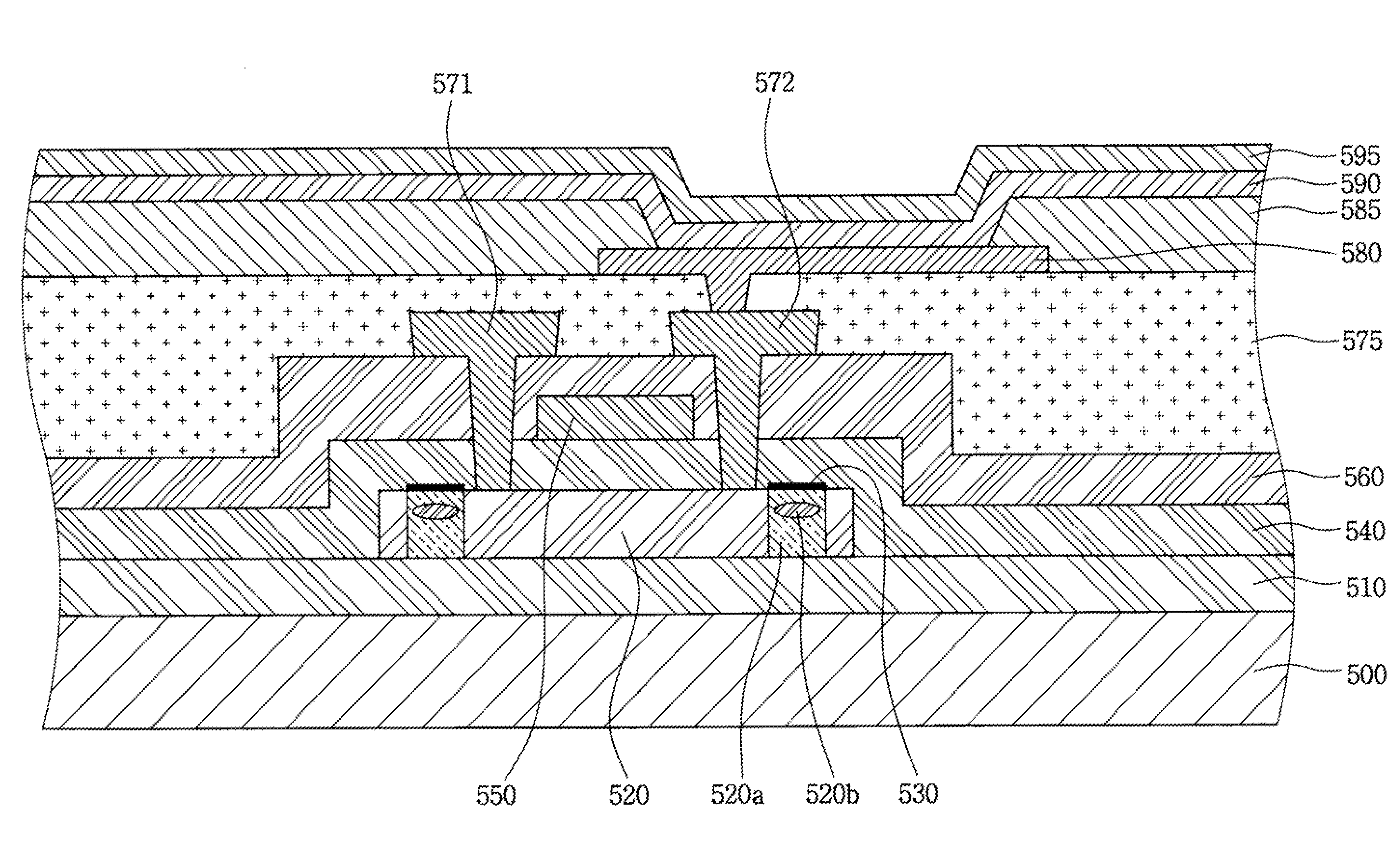
[0010]Aspects of the present invention provide a method of fabricating a polycrystalline silicon layer crystallized using crystallization-inducing metal by removing the crystallization-inducing metal remaining in a region of the polycrystalline silicon layer to be a channel, a thin film transistor (TFT) having a semiconductor layer formed of the polycrystalline silicon layer formed by the method so as to significantly lower leakage current, a method of fabricating the same, and an organic light emitting diode (OLED) display device using the same.

Problems solved by technology

However, SPC has disadvantages of a long processing time and a risk of transformation of the substrate due to the long processing time and high temperature used for the annealing.
ELC has disadvantages in that expensive laser equipment is required and interfacial characteristics between a semiconductor layer and a gate insulating layer may be poor due to protrusions generated on the created polycrystallized surface.
MIC and MILC have disadvantages in that a large amount of crystallization-inducing metal remains on the crystallized polycrystalline silicon layer to increase the leakage current of a semiconductor layer of a TFT.
However, methods of crystallization using a crystallization-inducing metal have a problem that characteristics of the TFT may deteriorate due to contamination by the crystallization-inducing metal.
However, even by these methods, the crystallization-inducing metals may not be effectively removed from the polycrystalline silicon layer, and high leakage current may still be a problem.

Method used


Image

  • Method of fabricating polycrystalline silicon layer, TFT fabricated using the same, method of fabricating TFT, and organic light emitting diode display device having the same
  • Method of fabricating polycrystalline silicon layer, TFT fabricated using the same, method of fabricating TFT, and organic light emitting diode display device having the same
  • Method of fabricating polycrystalline silicon layer, TFT fabricated using the same, method of fabricating TFT, and organic light emitting diode display device having the same

Examples


Embodiment Construction

[0027]Reference will now be made in detail to the present embodiments of the present invention, examples of which are illustrated in the accompanying drawings, wherein like reference numerals refer to the like elements throughout. The embodiments are described below in order to explain the present invention by referring to the figures.

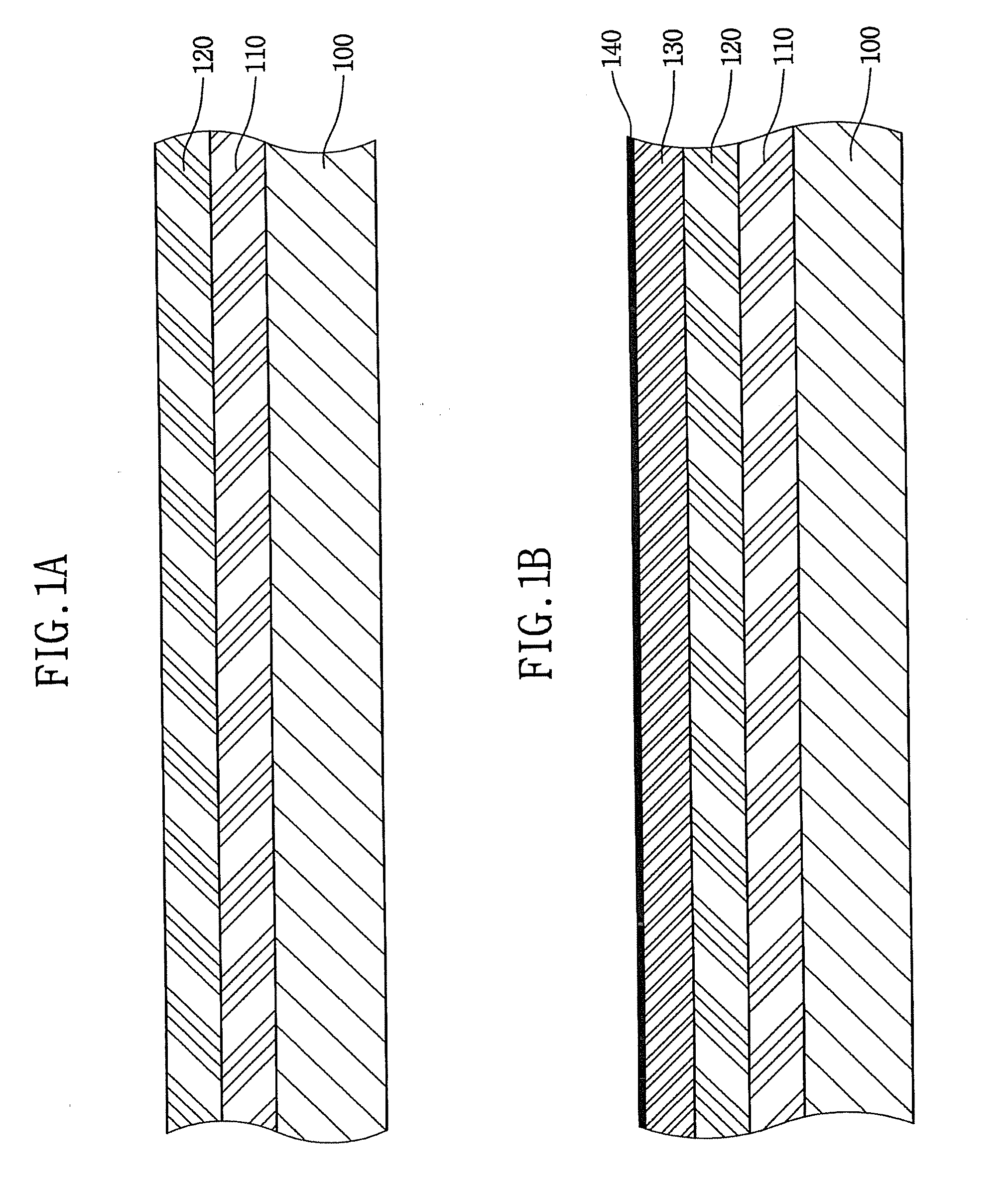
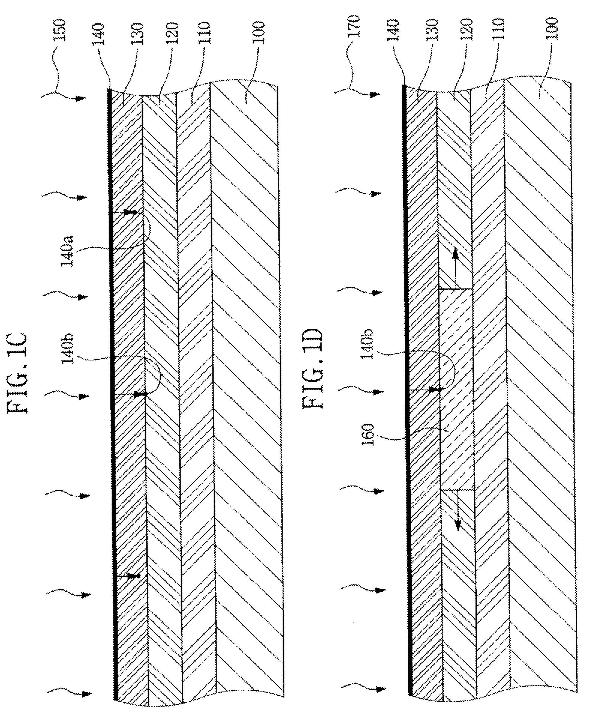
[0028]FIGS. 1A to 1D are cross-sectional views illustrating a crystallization process according to an embodiment of the present invention.

[0029]First, as illustrated in FIG. 1A, a buffer layer 110 may be formed on a substrate 100, which is formed of glass or plastic. The buffer layer 110 is an insulating layer and may be formed of silicon oxide, silicon nitride or a combination thereof by chemical vapor deposition (CVD) or physical vapor deposition (PVD). The buffer layer 110 serves to prevent the diffusion of moisture or impurities occurring in the substrate 100 or to adjust the heat transfer rate during crystallization, thereby allowing crystallizati...


PUM

PropertyMeasurementUnit
distanceaaaaaaaaaa
diffusion coefficientaaaaaaaaaa
temperatureaaaaaaaaaa

Abstract

A method of fabricating a polycrystalline silicon layer includes: forming an amorphous silicon layer on a substrate; crystallizing the amorphous silicon layer into a polycrystalline silicon layer using a crystallization-inducing metal; forming a metal layer pattern or metal silicide layer pattern in contact with an upper or lower region of the polycrystalline silicon layer corresponding to a region excluding a channel region in the polycrystalline silicon layer; and annealing the substrate to getter the crystallization-inducing metal existing in the channel region of the polycrystalline silicon layer to the region in the polycrystalline silicon layer having the metal layer pattern or metal silicide layer pattern. Accordingly, the crystallization-inducing metal existing in the channel region of the polycrystalline silicon layer can be effectively removed, and thus a thin film transistor having an improved leakage current characteristic and an OLED display device including the same can be fabricated.

Description

CROSS-REFERENCE TO RELATED APPLICATION[0001]This application claims the benefit of Korean Application No. 2007-53314, filed May 31, 2007, the disclosure of which is incorporated herein by reference.BACKGROUND OF THE INVENTION[0002]1. Field of the Invention[0003]Aspects of the present invention relate to a method of fabricating a polycrystalline silicon layer, a thin film transistor (TFT) fabricated using the same, a method of fabricating the TFT, and an organic light emitting diode (OLED) display device having the same. More particularly, aspects of the present invention relate to a method of fabricating a polycrystalline silicon layer, crystallized using crystallization-induced metal, wherein the method removes the crystallization-induced metal existing in a region of the polycrystalline silicon layer to be a channel by forming and annealing a metal layer or a silicide layer thereof. Aspects of the present invention further relate to a TFT having a semiconductor layer fabricated us...

Claims


Application Information

Patent Timeline
Patent Type & Authority Applications(United States)
IPC IPC(8): H01L51/52H01L21/322H01L29/786H01L21/336
CPCH01L21/02488H01L21/02532H01L21/02672H01L27/1277H01L29/66757H01L29/66765H01L29/78618H01L21/3221H01L21/3226H01L27/1214
Inventor PARK, BYOUNG-KEONSEO, JIN-WOOKYANG, TAE-HOONLEE, KIL-WONLEE, KI-YONG
Owner SAMSUNG MOBILE DISPLAY CO LTD
Learn More