Cdm ESD protection for integrated circuits

a protection circuit and integrated circuit technology, applied in the direction of emergency protection arrangements for limiting excess voltage/current, electrical apparatus, solid-state devices, etc., can solve the problems of destroying or impairing the function of the ics, requiring expensive repairs on the products, and not being tru

Inactive Publication Date: 2008-11-20
SOFICS BVBA
View PDF3 Cites 6 Cited by
  • Summary
  • Abstract
  • Description
  • Claims
  • Application Information

AI Technical Summary

Problems solved by technology

During installation of integrated circuits into products, these electrostatic discharges may destroy or impair the function of the ICs and thus require expensive repairs on the products, which could have been avoided by providing a mechanism for dissipation of the electrostatic discharge to which the IC may have been subjected.
The CDM threat in this patent is introduced because the functional device is placed directly in the substrate (not in an isolated well).
This is however not true.
Although the number of charges is limited, they can damage the gate oxide.

Method used


Image

  • Cdm ESD protection for integrated circuits
  • Cdm ESD protection for integrated circuits
  • Cdm ESD protection for integrated circuits

Examples


Embodiment Construction

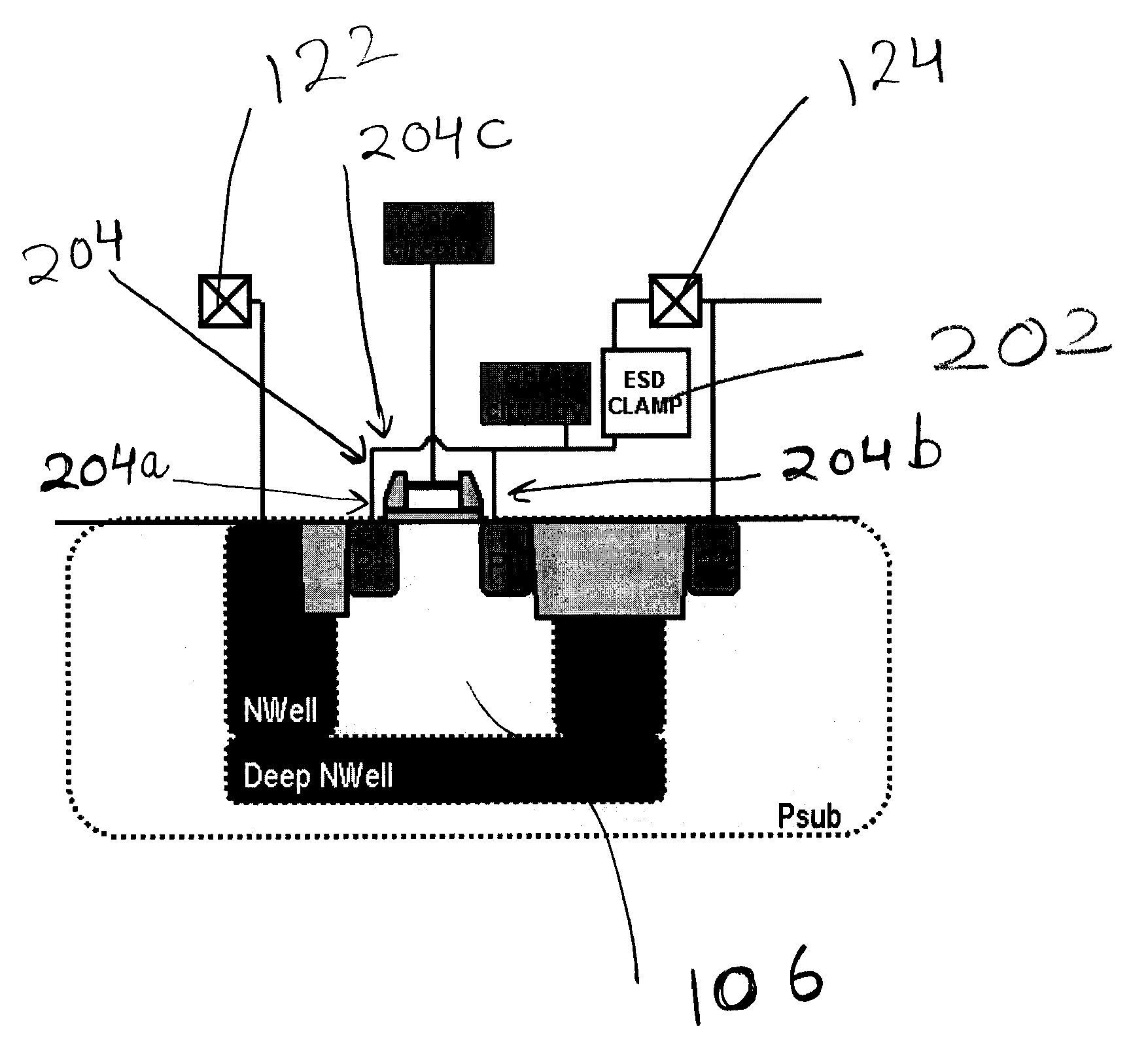
[0023]The invention relates to a technique to increase the CDM performance of an IC by connecting additional ESD clamps to isolated wells (or junctions). FIG. 2A illustrates a cross-section diagram of an Integrated Circuit IC 200 for CDM ESD protection in accordance with one embodiment of the present invention. The IC 200 illustrates a cross-section diagram of the transistor 104 formed in the isolated P-well region 106 with the deep N-well 108 and N-well 110 forming a ring structure around the isolated region to isolate / separate the P-well region 106 from the P-substrate 104. Furthermore, an additional ESD clamp 202 is coupled to the isolated P-well, 106 as shown in FIG. 2A. Specifically, the ESD clamp 202 is placed between the isolated P-well 106 and a reference node. The selection of the reference node depends on the normal operation requirements such as noise, cross-coupling, and other ESD elements. Preferably for ESD and in this example of FIG. 2A, the terminal to the isolated w...


PUM


Abstract

The present invention provides a charged-device model (CDM) electrostatic discharge (ESD) protection circuit for an integrated circuit (IC). The ESD protection circuit comprises a substrate of first conductivity type; a MOS component of second conductivity type formed on a first well on the substrate, and coupled to a pad; an isolating well/region having the second conductivity type being formed between the first well and the substrate to separate the first well and the substrate. Additionally, the circuit comprises an ESD clamp coupled to the isolated well/region. Under normal power operation, the ESD clamp is open. During a CDM ESD event, the CDM charges accumulated in the substrate and the MOS component are removed by the ESD clamp to prevent damage to the IC.

Description

FIELD OF THE INVENTION[0001]This invention generally relates to the field of electrostatic discharge (ESD) protection circuitry and, more specifically, improvements against Charged Device Model (CDM) stress cases in the protection circuitry of the integrated circuit (IC).BACKGROUND OF THE INVENTION[0002]Integrated circuits (ICs) and other semiconductor devices are extremely sensitive to the high voltages that may be generated by contact with an ESD event. As such, electrostatic discharge (ESD) protection circuitry is essential for integrated circuits. An ESD event commonly results from the discharge of a high voltage potential (typically, several kilovolts) and leads to pulses of high current (several amperes) of a short duration (typically, 100 nanoseconds). An ESD event can occur within an IC, illustratively, by human contact with the leads of the IC or by electrically charged machinery being discharged in other leads of an IC. During installation of integrated circuits into produ...

Claims


Application Information

Patent Timeline
Patent Type & Authority Applications(United States)
IPC IPC(8): H01L23/58H02H9/00
CPCH01L27/0251H01L2924/0002H01L2924/00
Inventor VAN CAMP, BENJAMINSORGELOOS, BART
Owner SOFICS BVBA
Why Eureka
Try Eureka