
Electroless plating apparatus with non-liquid heating source

a technology of electroless plating and heating source, which is applied in the direction of liquid/solution decomposition chemical coating, coating, basic electric elements, etc., can solve the problem that hot di water may develop an increasingly lower temperature along its path

Inactive Publication Date: 2008-10-30
TAIWAN SEMICON MFG CO LTD
View PDF10 Cites 7 Cited by
  • Summary
  • Abstract
  • Description
  • Claims
  • Application Information

AI Technical Summary

Benefits of technology

[0010]An advantageous feature of the embodiments of the present invention is that the plated wafers will have a substantially uniform temperature on their surfaces. Thus, the deposition rate across the wafer is more uniform. Also, the present invention provides the ability for adjusting the plating rates by adjusting the temperatures on wafers.

Problems solved by technology

However, in the conventional heating scheme, when hot DI wafer flows from the bottom center of wafer 2 to the edge, due to heat dissipation, the hot DI water may develop an increasingly lower temperature along its path.

Method used


Image

  • Electroless plating apparatus with non-liquid heating source
  • Electroless plating apparatus with non-liquid heating source
  • Electroless plating apparatus with non-liquid heating source

Examples


Embodiment Construction

[0018]The making and using of the presently preferred embodiments are discussed in detail below. It should be appreciated, however, that the present invention provides many applicable inventive concepts that can be embodied in a wide variety of specific contexts. The specific embodiments discussed are merely illustrative of specific ways to make and use the invention, and do not limit the scope of the invention.

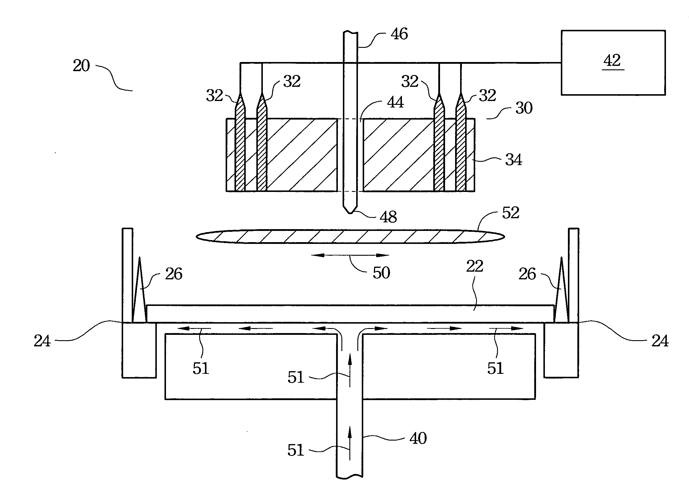
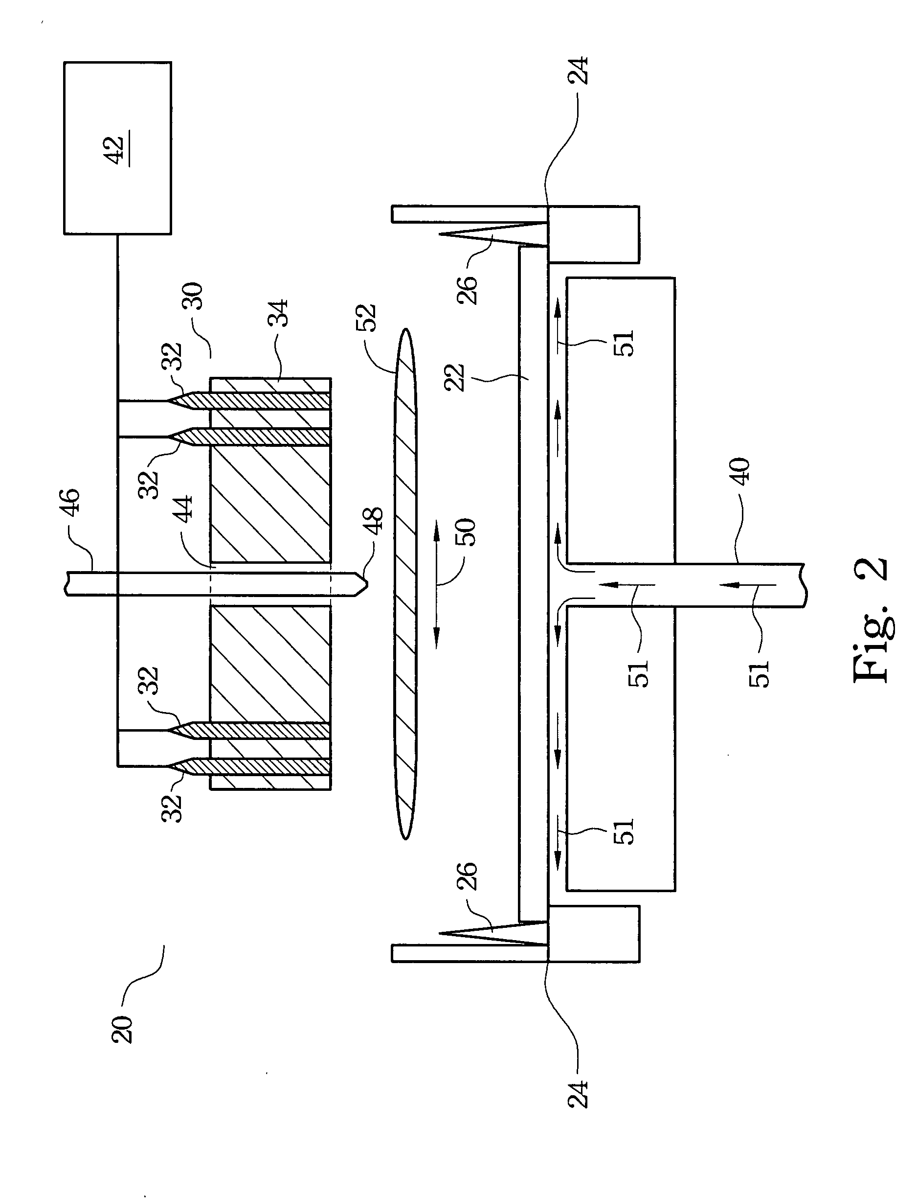
[0019]FIG. 2 schematically illustrates an exemplary electroless plating apparatus 20, which includes a radiation source 30 for providing heat to wafer 22. Wafer 22 is placed on wafer holder 24. Guide pins 26 in wafer holder 24 are used to confine wafer 22. In electroless plating processes, wafer holder 24 and wafer 22 swivel at a constant speed. Radiation source 30 may be any non-liquid heat source. For example, it may radiate any light with heating ability, such as infrared and / or far infrared lights. Radiation source 30 may include lamp filaments or coils.

[0020]In an exempl...


PUM

PropertyMeasurementUnit
temperatureaaaaaaaaaa

Abstract

An electroless plating apparatus is provided. The electroless plating apparatus includes a wafer holder; a chemical dispensing nozzle over the wafer holder; a conduit connected to the chemical dispensing nozzle; and a radiation source over the wafer holder.

Description

TECHNICAL FIELD[0001]This invention relates generally to methods and apparatus for electroless plating on semiconductor wafers, and more particularly to methods for controlling heating of semiconductor wafers during electroless plating in order to improve plating uniformity.BACKGROUND[0002]Electroplating and electroless plating can be used for the deposition of continuous metal layers as well as patterned metal layers. Electroless plating is often used as a preliminary step in preparing a seed layer for conventional electroplating. One of the process sequences used by the microelectronic manufacturing industry to deposit metals onto semiconductor wafers is known to as a “damascene” process. In such a process, via openings, trenches and / or other recesses, are formed in a dielectric layer and filled with a metal, such as copper. The wafer, with vias and trenches etched in the dielectric material, first receives a metallic seed layer, which is used to conduct electrical currents during...

Claims


Application Information

Patent Timeline
Patent Type & Authority Applications(United States)
IPC IPC(8): H01L21/3205B05B13/02
CPCC23C18/1216C23C18/1628C23C18/1667C23C18/1678H01L21/288H01L21/76873
Inventor CHAN, CHENG HSUNHWANG, CHIEN LING
Owner TAIWAN SEMICON MFG CO LTD
Learn More