
Semiconductor integrated circuit and method of controlling the same

a technology of integrated circuits and semiconductors, applied in the direction of digital storage, pulse techniques, and increasing the degree of modification, can solve the problems of increasing the influence of external noise, affecting the calibration process, and requiring a long time to perform calibration, so as to reduce the calibration time of odt resistance

Active Publication Date: 2008-10-16
SK HYNIX INC
View PDF8 Cites 15 Cited by
  • Summary
  • Abstract
  • Description
  • Claims
  • Application Information

AI Technical Summary

Benefits of technology

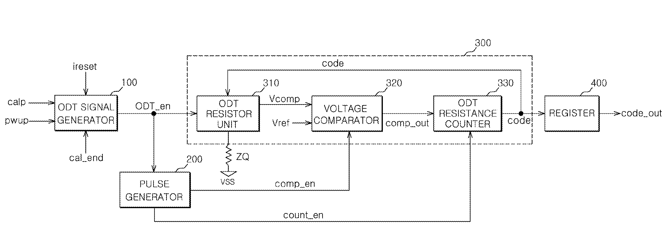
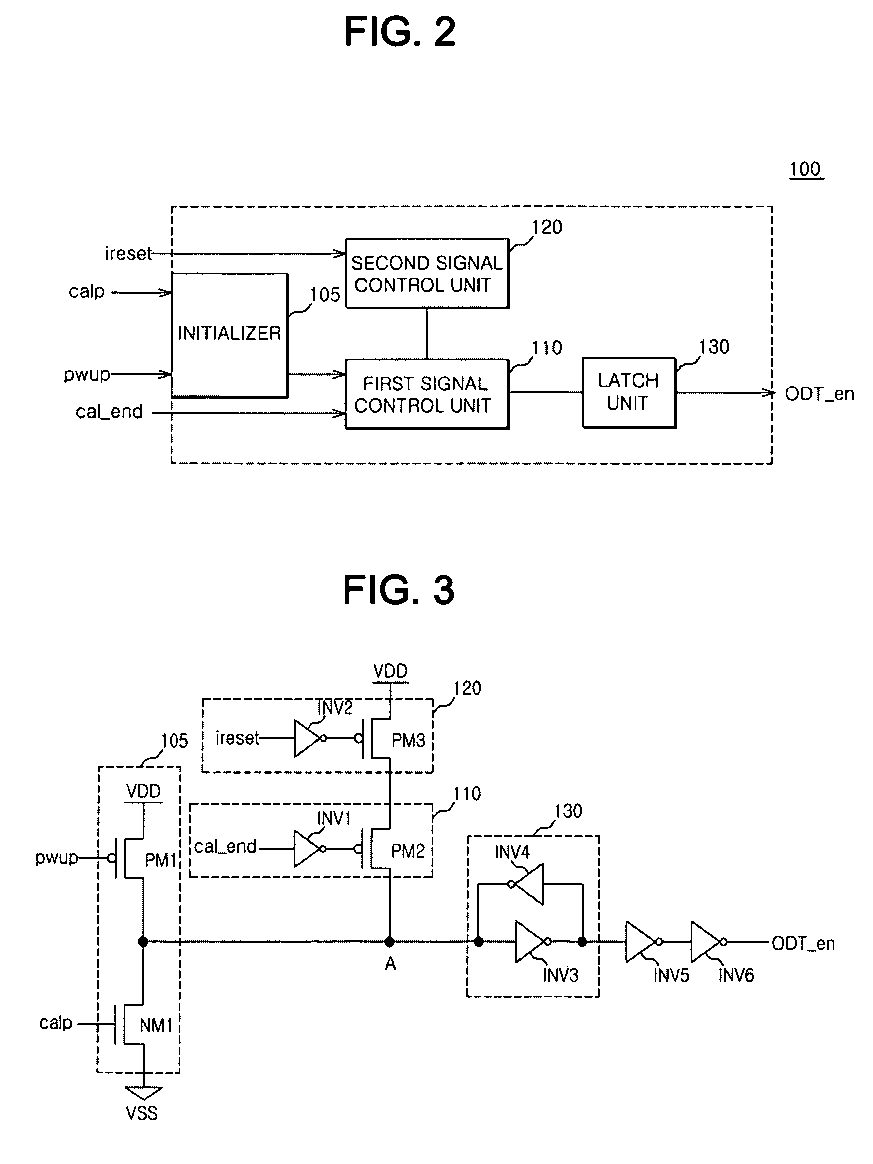
The invention provides a semiconductor integrated circuit and method for reducing the calibration time of ODT resistance. This is achieved by generating an ODT control signal based on an ODT command signal, an ODT reset signal, and an ODT calibration end signal. The ODT control signal activates an ODT resistor unit to perform an on-die termination operation. The semiconductor integrated circuit also includes an ODT signal generator, an ODT reset signal generator, a voltage comparator, a pulse generator, and an ODT resistance counter. The technical effect is to reduce the calibration time of ODT resistance and improve the efficiency of semiconductor integrated circuits.

Problems solved by technology

As the swing width of the signal is reduced, an influence on external noise increases.
That is, when a signal transmitted through a bus line having predetermined impedance passes through a bus line having different impedance, the signal may be partially reflected and then lost.
In particular, during the initial operation of the semiconductor integrated circuit, the resistance value of the ODT circuit is usually adjusted many times. Accordingly, it takes a lot of time to perform the calibration due to the repetition of activation and inactivation of the ODT resistor unit.
Further, while the ODT resistor unit is repeatedly activated and inactivated, a large amount of current may be consumed.

Method used


Image

  • Semiconductor integrated circuit and method of controlling the same
  • Semiconductor integrated circuit and method of controlling the same
  • Semiconductor integrated circuit and method of controlling the same

Examples


Embodiment Construction

[0020]The attached drawings for illustrating preferred embodiments of the present invention are referred to in order to gain a sufficient understanding of the present invention, the merits thereof, and the objectives accomplished by the implementation of the present invention.

[0021]Hereinafter, an exemplary embodiment of the invention will be described with reference to the accompanying drawings.

[0022]An exemplary embodiment of the present invention provides a semiconductor integrated circuit that can reduce a calibration time of ODT resistance. In particular, during a period in which an ODT calibration end signal is inactivated, a control is performed such that an ODT control signal can be continuously activated. Accordingly, while the ODT calibration end signal is inactivated, repetitive activation and inactivation of an ODT resistor unit is not performed. Therefore, the calibration time of ODT resistance can be reduced. Further, current consumption can be reduced.

[0023]A semicond...


PUM


Abstract

A semiconductor integrated circuit includes an ODT signal generator that receives an ODT command signal, an ODT reset signal, and an ODT calibration end signal to generate an ODT control signal according to the phase of the ODT calibration end signal, and an ODT resistance adjusting unit that is to perform an on-die termination operation in response to the ODT control signal.

Description

CROSS-REFERENCE TO RELATED APPLICATION[0001]This application claims priority from Korean Patent Application No. 10-2007-0035488 filed on Apr. 11, 2007 in the Korean Intellectual Property Office, the disclosure of which is incorporated herein by reference in its entirety.BACKGROUND OF THE INVENTION[0002]1. Technical Field[0003]The present invention relates to a semiconductor integrated circuit, and in particular, to an on-die termination circuit.[0004]2. Related Art[0005]In recent years, due to a high operation speed of electronic devices, the swing width of a signal is reduced in order to minimize a transmission time of an interface signal between semiconductor apparatuses. As the swing width of the signal is reduced, an influence on external noise increases. That is, when a signal transmitted through a bus line having predetermined impedance passes through a bus line having different impedance, the signal may be partially reflected and then lost. This phenomenon is called impedance...

Claims


Application Information

Patent Timeline
Patent Type & Authority Applications(United States)
IPC IPC(8): H03K17/16
CPCH03K19/0002G11C7/10
Inventor LEE, JUN WOOKIM, KYUNG HOON
Owner SK HYNIX INC
Learn More