Transmissive active grating device

Inactive Publication Date: 2008-10-02
SAMSUNG ELECTRONICS CO LTD
View PDF1 Cites 0 Cited by
  • Summary
  • Abstract
  • Description
  • Claims
  • Application Information

AI Technical Summary

Benefits of technology

[0010]Exemplary embodiments of the present invention provide a transmissive active grating device that is formed by a simple fabrication process, and which does not involve mechanical movement, and provide a transmissive active grating device having a high response speed.

Problems solved by technology

However, the conventional reflective active grating device 10 is a three-dimensional structure involving a mechanical movement, and thus, conventional reflective active grating device 10 must undergo a micro-electro-mechanical system (MEMS) process which is a very delicate process.
Moreover, since the conventional reflective active grating device 10 reflects the incident light, the light path is bent and the optical system becomes complex.

Method used


Image

  • Transmissive active grating device
  • Transmissive active grating device
  • Transmissive active grating device

Examples


Embodiment Construction

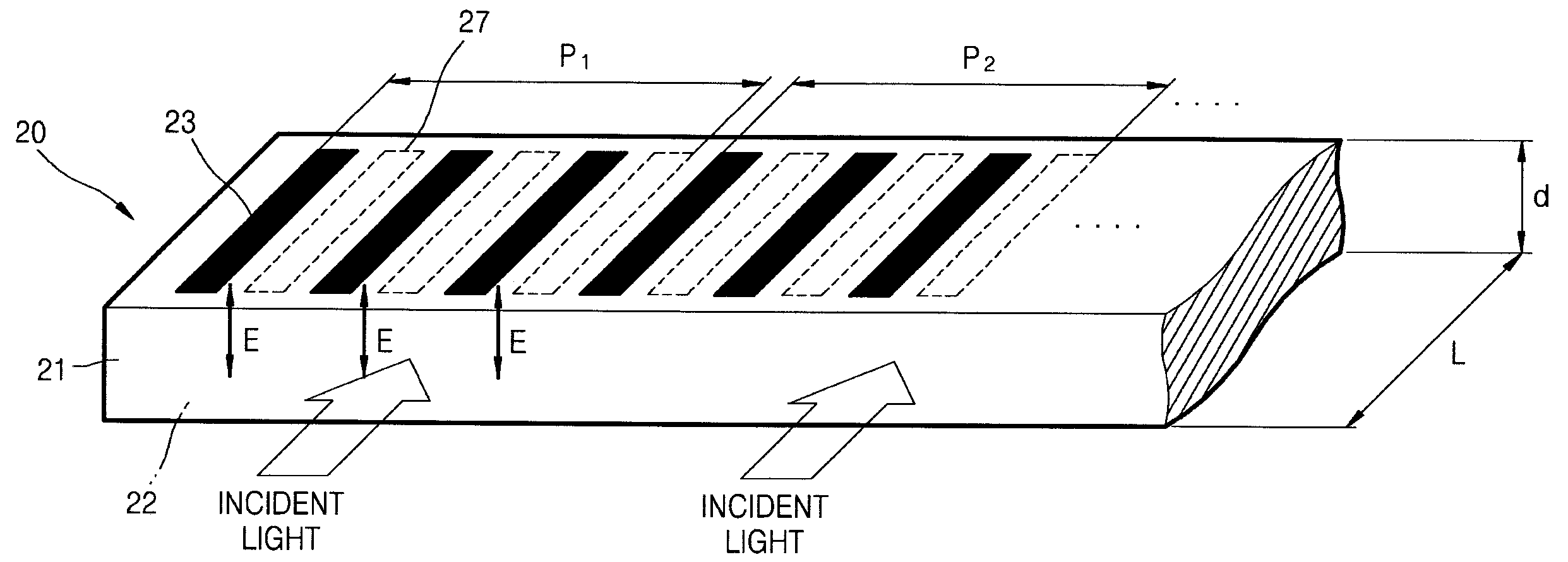
[0029]FIG. 4 is a perspective view showing a conceptual structure of a transmissive active grating device 20 according to an exemplary embodiment of the present invention. Referring to FIG. 4, the transmissive active grating device 20 according to the current embodiment includes a light transmissive electro optical material layer 21, a common electrode 22 formed on a bottom surface of the electro optical material layer 21, and an array of a plurality of grating electrodes 23 arranged in parallel with each other on a top surface of the electro optical material layer 21. As denoted by an arrow in FIG. 4, the light is incident onto and exits through side surfaces of the electro optical material layer 21, on which the common electrode 22 and the grating electrodes 23 are not formed.

[0030]The electro optical material layer 21 can be formed of an electro optical crystal that transmits the light and has a refractive index changed by an electric field. The electro optical crystal has a refr...


PUM


Abstract

Provided is a transmissive active grating device that transmits light or diffracts light according to an applied voltage. The transmissive active grating device includes: an electro optical material layer which transmits light; a first electrode formed on a bottom surface of the electro optical material layer; and an array of a plurality of second electrodes arranged on a top surface of the electro optical material layer in parallel with each other.

Description

CROSS-REFERENCE TO RELATED PATENT APPLICATIONS[0001]This application claims priority from Korean Patent Application No. 10-2007-0030034, filed on Mar. 27, 2007, in the Korean Intellectual Property Office, the disclosure of which is incorporated herein in its entirety by reference.BACKGROUND OF THE INVENTION[0002]1. Field of the Invention[0003]Apparatuses consistent with the present invention relate to a transmissive active grating device, and more particularly, to a transmissive active grating device transmitting or diffracting a light according to an applied voltage.[0004]2. Description of the Related Art[0005]Active grating devices, which perform as gratings for diffracting light according to an applied voltage, are combined with optical systems in order to be used as light modulators in laser printers or display devices.[0006]FIG. 1 is a perspective view of a conventional reflective active grating device 10. Referring to FIG. 1, the conventional reflective active grating device 1...

Claims


Application Information

Patent Timeline
IPC IPC(8): G02F1/29
CPCB41J2/465G02F1/292G02F2203/12G02B26/00B81B7/00
Inventor MOON, YONG-KWEUNWON, JONG-HWA
Owner SAMSUNG ELECTRONICS CO LTD
Why Eureka
Try Eureka