


Quick Research
Generate reliable direction feasibility study reports for your R&D in just a few steps.

Technical Q&A
Discover and master advanced knowledge NOW. Basics, ideas, possibilities, all at once.

Find Solutions
As an expert in R&D theories, this can generate solutions to your technical problems instantly.

Evaluate Feasibility
Analyze your overall solution with one click, know your potential R&D risks in advance.

Monitor Landscape
Get weekly tech updates, stay abreast of the latest tech innovations and key insights.
Composite Quantum Dot Structures
a quantum dot and composite technology, applied in the field of quantum dot structure, can solve the problems of reducing the flexibility of the design assumed by the prior art, affecting the implementation of the prior art to optoelectronic devices, and unable to optimise the ensemble of quantum dots with such thin layers
- Summary
- Abstract
- Description
- Claims
- Application Information
AI Technical Summary
Benefits of technology
Problems solved by technology
Method used
Image

Examples
first embodiment
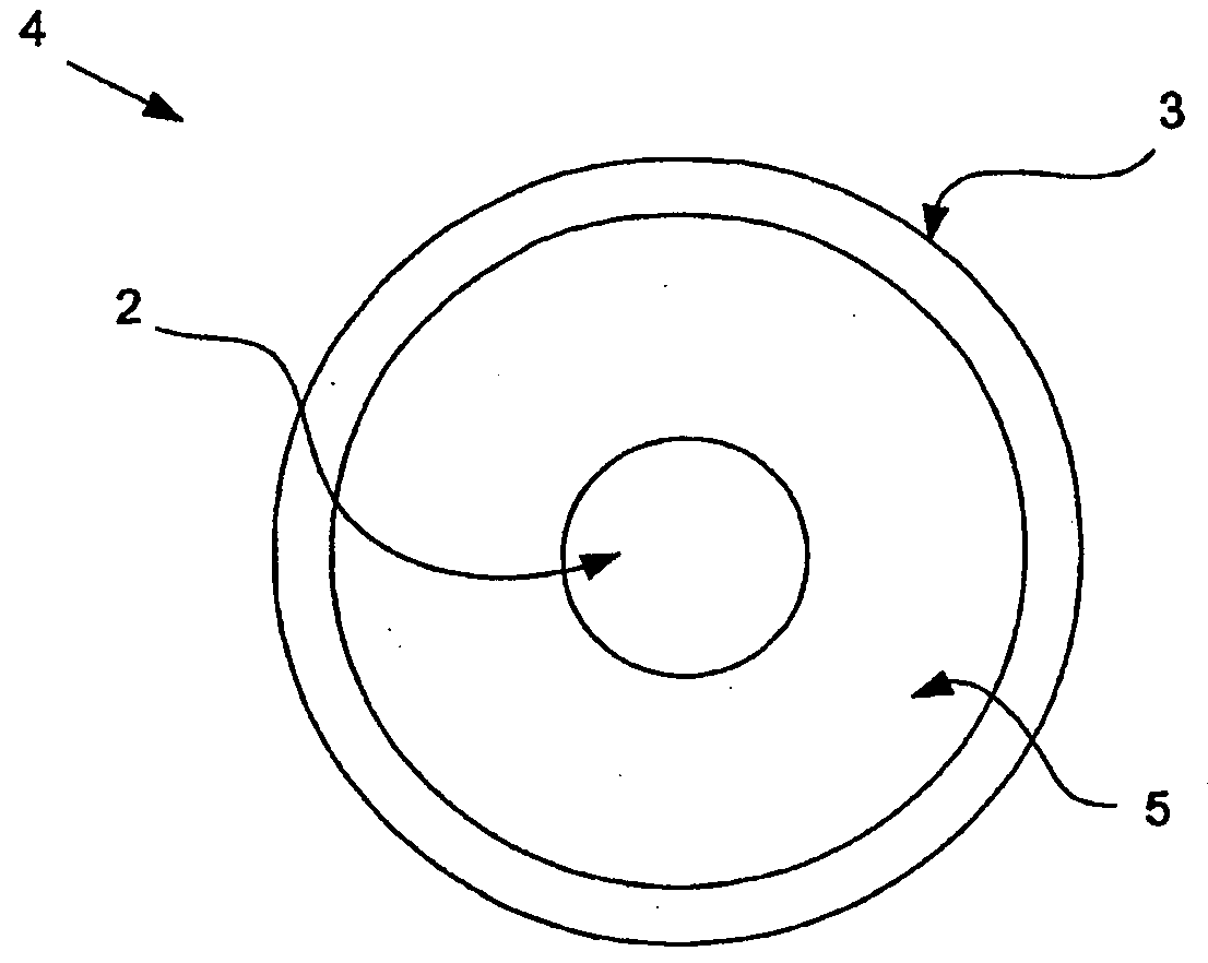
[0045]Referring to FIG. 3, a quantum dot structure 4 according to the invention is provided in a “scotch egg” type structure, with a barrier layer 5, provided between a quantum dot 2 and a metal layer 3. The barrier layer 5 prevents charge carriers, in other words, electrons and / or holes, from leaving the quantum dot 2.
[0046]The invention allows the radius of the quantum dot 2 to be chosen to display the desired optoelectronic property required, such as absorption / gain at particular wavelengths. As noted previously, the radius of the quantum dot 2 would typically be 5 nm or less. The outer radius of the barrier layer 5 may be typically 10 times bigger than the radius of the quantum dot 2, and is preferably chosen to maximise the electric field in the quantum dot 2 while, at the same time, being large enough so that the required width of the metal layer 3 can be reliably deposited.
[0047]In an ensemble of such quantum dot structures 4, the required width of the metal layer 3 may be su...
third embodiment
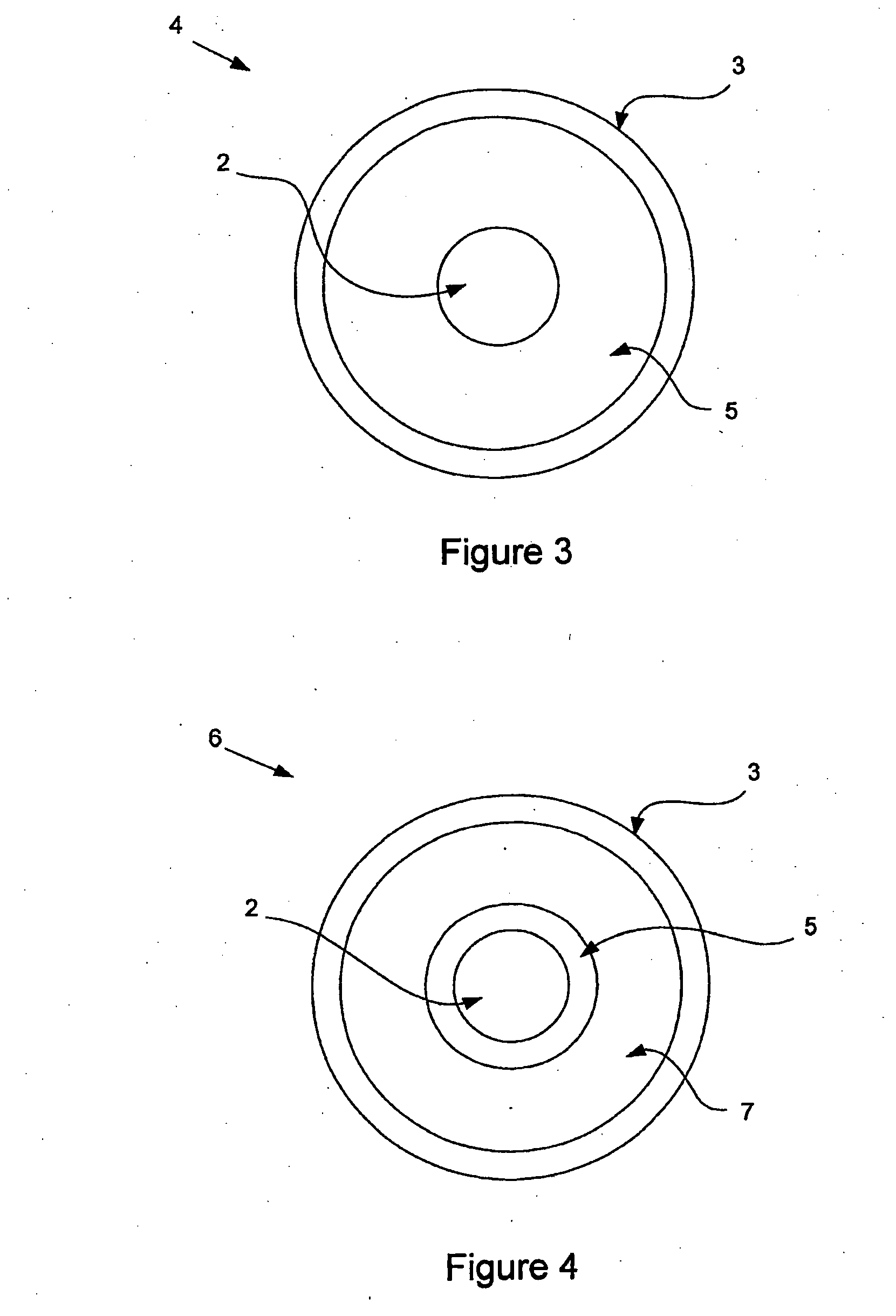
[0056]FIG. 5 depicts a quantum dot structure 8 according to the invention, comprising a barrier 5, surrounded by a charge carrier confinement region 2 and a metal layer 3. In order to prevent charge carriers entering the barrier 5, the barrier 5 is formed of a material with a band gap that is wider than that of the material used to form the charge carrier confinement region 2. The metal layer 3 also acts to wholly or substantially confine the charge carriers to the charge carrier confinement region 2.
fourth embodiment
[0057]FIG. 6 depicts a quantum dot structure 9 according to the invention. In a similar manner to the quantum dot structure 8 of FIG. 5, the quantum dot structure 9 comprises a barrier 5 surrounded by a charge carrier confinement region 2. One or more cladding layers 7 are provided between the charge carrier confinement region 2 and the metal layer 3, in order to compensate for any lack of chemical affinity between the charge carrier confinement region 2 and metal layer 3. The combination of the cladding layer 7 and the metal layer 3 also act to wholly or substantially confine the charge carriers to the charge carrier confinement region 2.
[0058]As described above in relation to the first embodiment, the dimensions of the charge carrier confinement region 2 are selected so that the quantum dot structure provides the desired optical properties, while the dimensions of the barrier 5 are chosen so that the combined dimensions of the charge carrier confinement region and the barrier 5 ar...
PUM
 Abstract
Description
Claims
Application Information
 - R&D Engineer
- R&D Manager
- IP Professional
- Industry Leading Data Capabilities
- Powerful AI technology
- Patent DNA Extraction
Browse by: Latest US Patents, China's latest patents, Technical Efficacy Thesaurus, Application Domain, Technology Topic, Popular Technical Reports.
© 2024 PatSnap. All rights reserved.Legal|Privacy policy|Modern Slavery Act Transparency Statement|Sitemap|About US| Contact US: help@patsnap.com