Electrostatic discharge protection component, and electronic component module using the same
a technology of electrostatic discharge and protection component, applied in the direction of emergency protective circuit arrangement, emergency protective arrangement for limiting excess voltage/current can solve problems such as occurrence of problems, electronic equipment, electronic components, etc., to efficiently dissipate heat generated, excellent resistance to electrostatic discharge pulses, and efficient dissipation
- Summary
- Abstract
- Description
- Claims
- Application Information
AI Technical Summary
Benefits of technology
Problems solved by technology
Method used
Image

Examples
exemplary embodiment 1
[0040]A protection component and a light-emitting diode module in the exemplary embodiment 1 of the present invention will be described in the following.
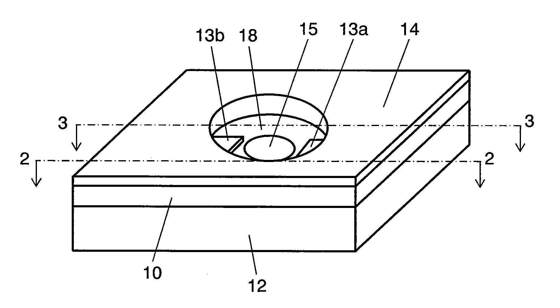
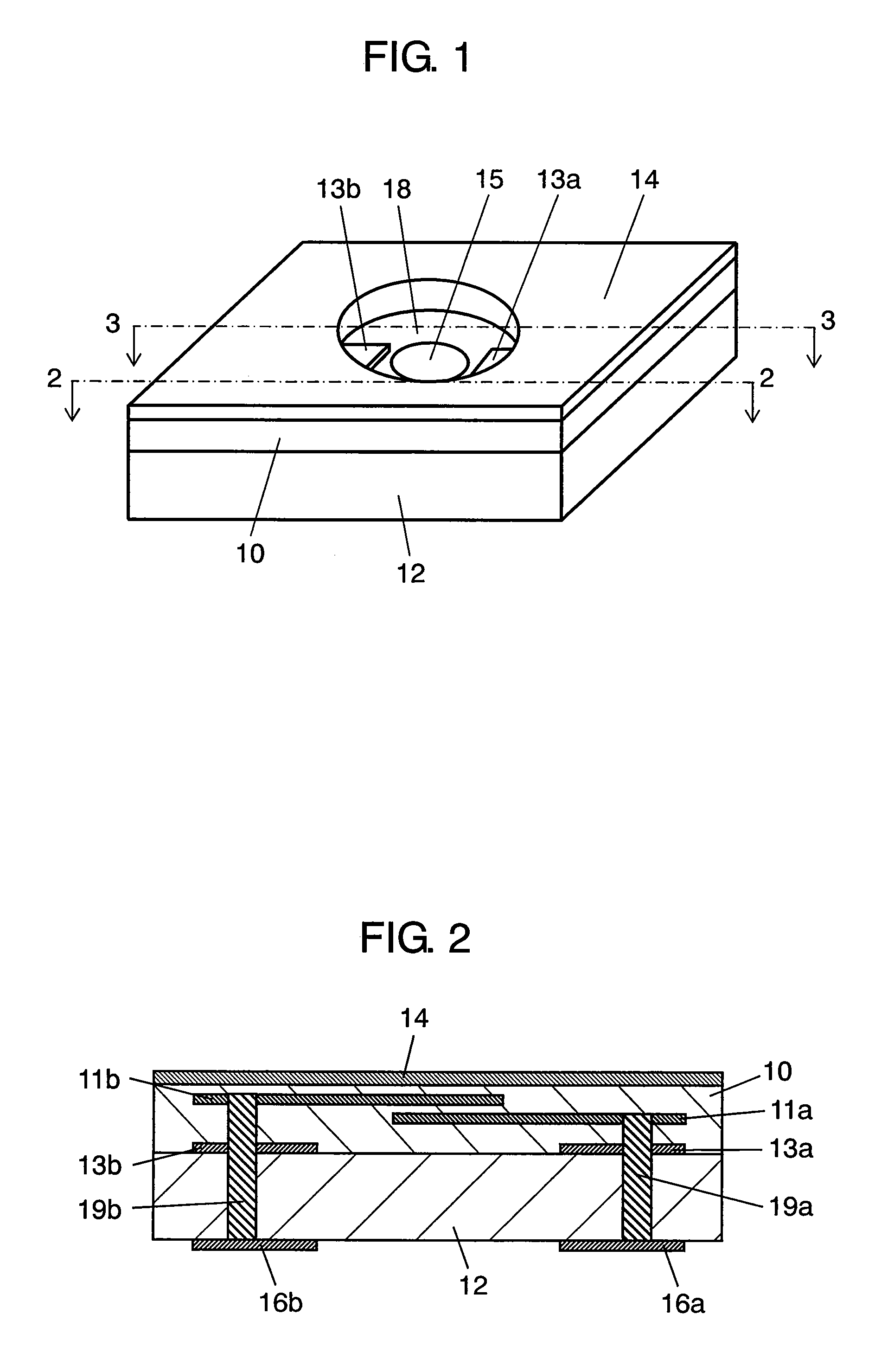
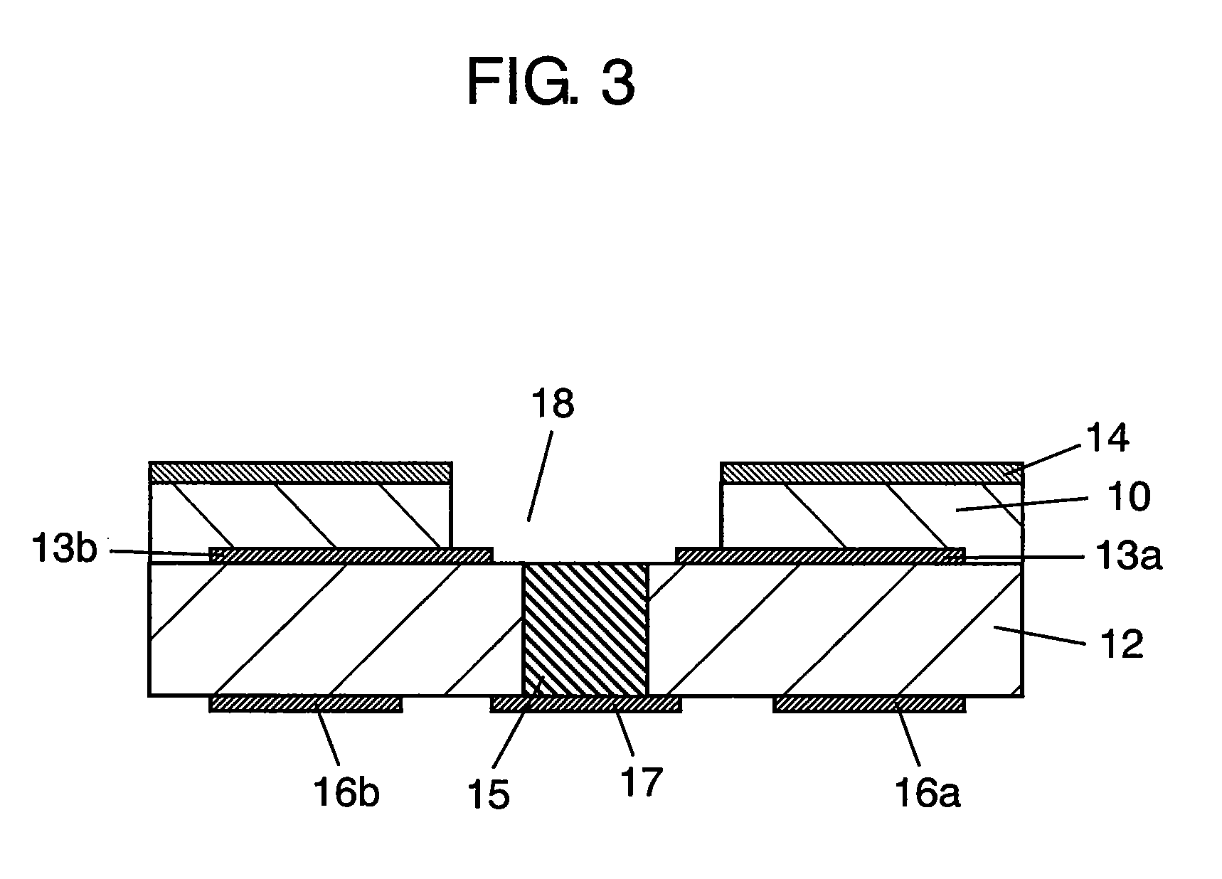
[0041]FIG. 1 is a perspective outline view of a protection component in the exemplary embodiment 1 of the present invention. FIG. 2 is a sectional view along 2-2 line of the protection component in the exemplary embodiment. FIG. 3 is a sectional view along 3-3 line of the protection component in the exemplary embodiment. FIG. 4 is a schematic exploded perspective view of the protection component in the exemplary embodiment. FIG. 5 is a sectional view of a light-emitting diode module in the exemplary embodiment. FIG. 6 is an equivalent circuit diagram of the light-emitting diode module in the exemplary embodiment.
[0042]As shown in FIGS. 1 to 4, a protection component in the exemplary embodiment includes varistor portion 10 formed by alternately laminating three varistor layers 10a, 10b and 10c, internal electrodes 11a and 11b. Furthe...
exemplary embodiment 2
[0074]A protection component and light-emitting diode module in the exemplary embodiment 2 of the present invention will be described in the following.
[0075]The point of difference between the exemplary embodiment 2 and the exemplary embodiment 1 is such that in the exemplary embodiment 1, external electrodes 16a, 16b are formed on the surface where terminal electrodes 13a, 13b of ceramic substrate 12 are formed, while in the exemplary embodiment 2, external electrodes 16a, 16b are formed on the side surface of varistor portion 10 and ceramic substrate 12.
[0076]FIG. 12 is an outline perspective view of a protection component in the present exemplary embodiment. FIG. 13 is a sectional view along 13-13 line in FIG. 12 of the protection component in the present exemplary embodiment. FIG. 14 is a sectional view along 14-14 line in FIG. 12 of the protection component in the present exemplary embodiment. FIG. 15 is a schematic exploded perspective view of the protection component in the p...
PUM
| Property | Measurement | Unit |
|---|---|---|
| thickness | aaaaa | aaaaa |
| diameter | aaaaa | aaaaa |
| thickness | aaaaa | aaaaa |
Abstract
Description
Claims
Application Information
 - R&D
- Intellectual Property
- Life Sciences
- Materials
- Tech Scout
- Unparalleled Data Quality
- Higher Quality Content
- 60% Fewer Hallucinations
Browse by: Latest US Patents, China's latest patents, Technical Efficacy Thesaurus, Application Domain, Technology Topic, Popular Technical Reports.
© 2025 PatSnap. All rights reserved.Legal|Privacy policy|Modern Slavery Act Transparency Statement|Sitemap|About US| Contact US: help@patsnap.com