
Low Capacitance Transient Voltage Suppressor

a transient voltage suppressor, low capacitance technology, applied in the direction of diodes, semiconductor devices, electrical apparatus, etc., can solve the problems of power and therefore could be destroyed, damage or destroy severely electronic systems, damage to voltage spikes, etc., to achieve the effect of low capacitan

Inactive Publication Date: 2008-09-11
PROTEK DEVICES
View PDF3 Cites 12 Cited by
  • Summary
  • Abstract
  • Description
  • Claims
  • Application Information

AI Technical Summary

Benefits of technology

[0013]The invention combines a PIN diode with a PN transient voltage suppressor diode to create a unique family of low capacitance transient voltage suppressors. The PIN diode and the PN diode are connected in a back-to-back configuration and housed in the same package thereby forming a transient voltage suppressor that controls positive voltage spikes above a specified threshold. This type of transient voltage suppressor is called a uni-directional device. It is also possible to house two (2) PIN diodes and two (2) PN diodes suitable connected within a single package whereby that combination provides protection for both positive and negative voltage spikes. This type of transient voltage suppressor is called a bi-directional device.

Problems solved by technology

This breakdown voltage is a critical point since the PN diode is operating at both high voltage and high current, it is experiencing high power and therefore could be destroyed if such high power conditions lasted for a substantial period of time.
One such application that was needed early on was transient voltage suppressor since high voltage spikes could severely damage or destroy electronic systems.
This problem was noted early on in telephone systems, which were hit by lightening strikes causing the damaging voltage spikes.
As solid state electronics evolved getting faster, smaller and operating at lower voltage levels, problems with voltage transients increased.
Now along with problems of surges in the power lines due to a variety of causes, the solid-state electronic devices had problems with electro-static discharge again due to a variety of causes, but often associated with handling of the electronic device or system.
One electrical characteristic that created challenges for the makers of transient voltage suppressors is the capacitance associated with the suppressor, which caused problems in the system in which the suppressor was installed.
It is difficult to reduce the capacitance of a transient voltage suppressor PN diode since that capacitance is related directly to the active area of the PN diode.
Obviously this circuit can only protect against voltage transients in one direction.
As can be readily understood, the PIN diode is not an efficient rectifier or other general purpose diode since the intrinsic layer causes a great deal of resistance which in turn causes significant loss of useful power.
This power goes into heat and cannot be used by the remainder of any electronic circuit.
The ongoing problem is that as electronic circuits get faster, they also get more sensitive to smaller amounts of over voltage and need better protection than is supplied by available voltage transient suppressors.
In addition, these advanced, high speed circuits need to have a very low capacitance associated with a voltage transient suppressor since any such capacitance can slow down the performance of that high-speed circuit.
There is no commercially available voltage transient suppressor technology that can provide the needed protection for such high-speed circuits.

Method used


Image

  • Low Capacitance Transient Voltage Suppressor
  • Low Capacitance Transient Voltage Suppressor
  • Low Capacitance Transient Voltage Suppressor

Examples


Embodiment Construction

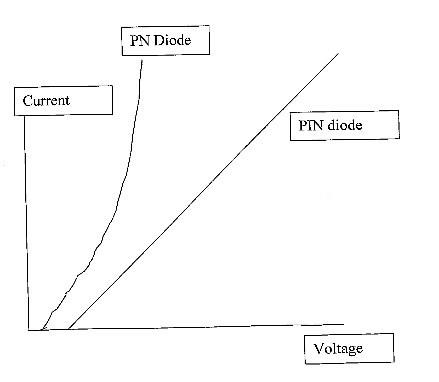
[0018]FIG. 1 shows the construction of a PN diode 10 where the P-type region 11 is in direct contact with the N-type region 12 within the semiconductor material 14. This contact is called the PN junction 13 where the junction 13 controls much of the electrical performance of the resulting device. The theory of the PN junction 13 and the manufacturing technology for such PN diodes 10 is well known and well established with many variations possible. The limitation to PN diodes 10 is that the area of such a device must be increased to increase the ability for that PN diode 10 to absorb power, which is critical in transient voltage suppressors. Increasing the area of a PN diode 10 also increases the capacitance associated with that diode.

[0019]FIG. 2 shows the more complex structure of a PIN diode 20 where the P-type region 11 is now in direct contact with an intrinsic region 21 while the N-type region 12 is also in contact with the opposite side of that intrinsic region 21. This struct...


PUM


Abstract

A transient voltage suppressor includes a reverse bias transient voltage suppressor PN diode connected in series with a forward biased PIN diode, the series circuit formed by the PN diode and the PIN diode is connected between first and second terminals and in parallel with a reverse biased PIN diode.

Description

FIELD OF THE INVENTION[0001]This invention is in the field of solid state device circuits and particularly in the field of diode based transient voltage suppressor circuitsBACKGROUND[0002]The PN diode where a P-type impurity is incorporated into semiconductor material along with N-type impurity remains an important device. A P-type impurity is one where there is an excess of holes or what are treated as positive, mobile charges hence the P for positive while an N-type impurity is where there are an excess of negative, mobile charges hence the N for negative. The key to the electrical performance of the PN diode is the junction where the P-type and N-type impurities are the same concentration in the semiconductor material. At either side of this point the semiconductor material is either P-type or N-type. This structure can be realized in many ways but in every case the PN diode has very similar current-voltage characteristics. In a forward-biased condition where an outside voltage i...

Claims


Application Information

Patent Timeline
IPC IPC(8): H01L29/868
CPCH01L27/0255
Inventor MATTESON, FREDKANSAL, RAKESH
Owner PROTEK DEVICES
Learn More