Remote bist for high speed test and redundancy calculation

a bist and high-speed technology, applied in the field of bist architectures, can solve problems such as large amount of chip real estate, and achieve the effect of high-speed testing and minimal width

Inactive Publication Date: 2008-09-04
META PLATFORMS INC
View PDF0 Cites 389 Cited by
  • Summary
  • Abstract
  • Description
  • Claims
  • Application Information

AI Technical Summary

Benefits of technology

[0008]Disclosed in a hybrid built-in self test (BIST) architecture for embedded memory arrays that segments BIST functionality into remote lower-speed executable instructions and local higher-speed executable instructions. A standalone BIST logic controller operates at a lower frequency and communicates with a plurality of embedded memory arrays using a BIST instruction set. A block of higher-speed test logic is incorporated into each embedded memory array under test and this higher-speed test logic locally processes BIST instructions received from the standalone BIST logic controller at a higher frequency. The higher-speed test logic can include a clock multiplier for increasing the processing frequency of the BIST instructions and logic that acts as an instruction multiplier for converting the BIST instructions from the lower frequency to the higher frequency. The standalone BIST logic controller enables a plurality of higher-speed test logic structures in a plurality of embedded memory arrays.
[0013]The remote BIST architecture allows for one BIST to interact with a series of embedded memories through a set of complex macro instructions running at low frequency. Each embedded memory macro has a local block of high speed test logic which produces the high speed micro instructions for correctly stimulating the embedded memory array at high speed. The architecture allows for a simple low speed bus of minimal width to allow communication between the remote BIST and the embedded memory macros. Also, this architecture provides for flexible, high speed testing of multiple embedded memory macros simultaneously.

Problems solved by technology

To associate a BIST with each memory array would consume a considerable amount of chip real estate.

Method used


Image

  • Remote bist for high speed test and redundancy calculation
  • Remote bist for high speed test and redundancy calculation
  • Remote bist for high speed test and redundancy calculation

Examples


Embodiment Construction

[0018]The present invention and the various features and advantageous details thereof are explained more fully with reference to the nonlimiting embodiments that are illustrated in the accompanying drawings and detailed in the following description. It should be noted that the features illustrated in the drawings are not necessarily drawn to scale. Descriptions of well-known components and processing techniques are omitted so as to not unnecessarily obscure the present invention. The examples used herein are intended merely to facilitate an understanding of ways in which the invention may be practiced and to further enable those of skill in the art to practice the invention. Accordingly, the examples should not be construed as limiting the scope of the invention.

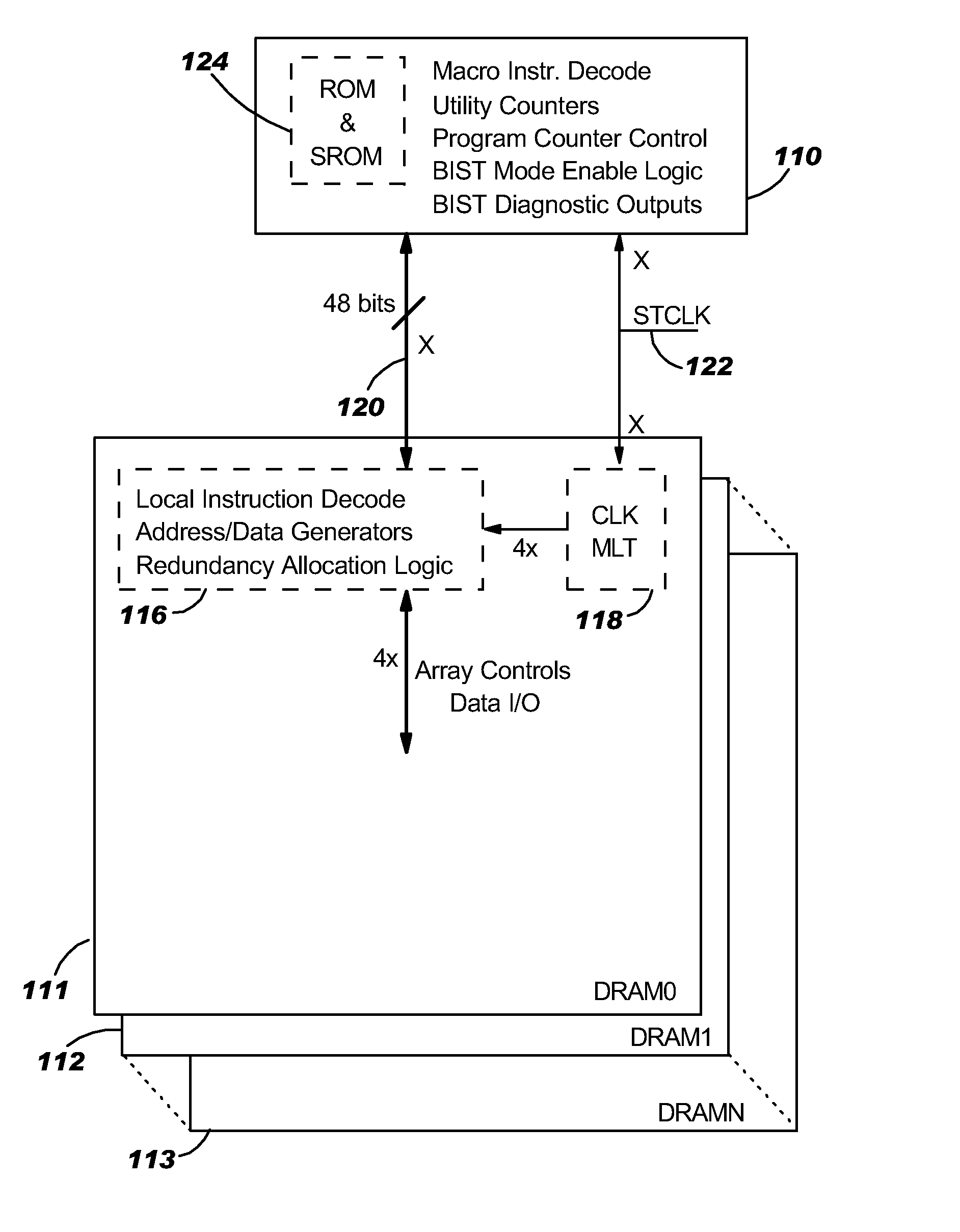
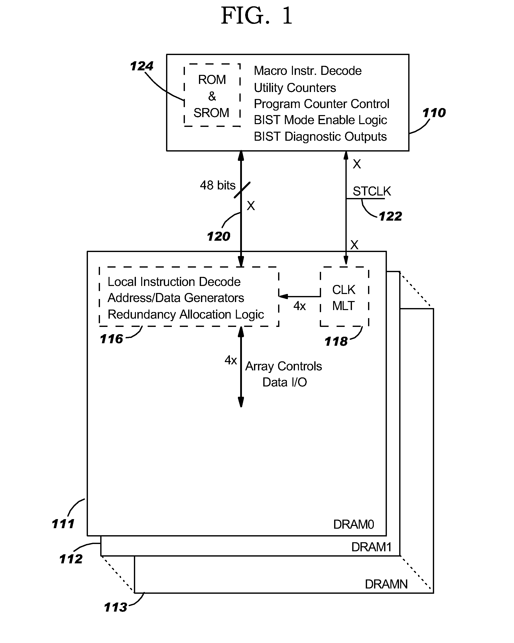
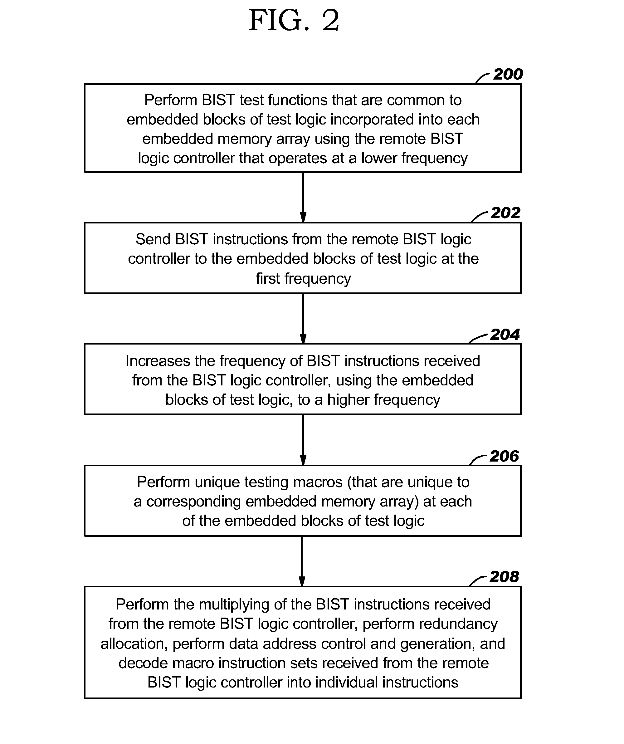
[0019]As shown in greater detail below, the invention provides a remote built-in self test device for testing a plurality of embedded memories, whereby the BIST operates at a low frequency and communicates with the multiple ...


PUM


Abstract

Disclosed in a hybrid built-in self test (BIST) architecture for embedded memory arrays that segments BIST functionality into remote lower-speed executable instructions and local higher-speed executable instructions. A standalone BIST logic controller operates at a lower frequency and communicates with a plurality of embedded memory arrays using a BIST instruction set. A block of higher-speed test logic is incorporated into each embedded memory array under test and locally processes BIST instructions received from the standalone BIST logic controller at a higher frequency. The higher-speed test logic includes a multiplier for increasing the frequency of the BIST instructions from the lower frequency to the higher frequency. The standalone BIST logic controller enables a plurality of higher-speed test logic structures in a plurality of embedded memory arrays.

Description

CROSS-REFERENCE TO RELATED APPLICATIONS[0001]This application is a continuation of U.S. application Ser. No. 10 / 707,971 filed Jan. 29, 2004, the complete disclosure of which, in its entirety, is herein incorporated by reference.BACKGROUND OF THE INVENTION[0002]1. Field of the Invention[0003]The present invention relates to BIST architectures and more particularly, to an architecture for embedded memory arrays that segments BIST functionality into remote lower-speed executable instructions and local higher-speed executable instructions.[0004]2. Description of the Related Art[0005]As embedded memory sizes continue to increase, overall BIST testing time will also increase; hence, novel schemes that reduce testing time while maintaining test integrity and diagnostic resolution are of great value.[0006]In current and future designs, there is a need to separate and distribute memory arrays across a die, placing them near the functional units that they are associated with. To associate a B...

Claims


Application Information

Patent Timeline
Patent Type & Authority Applications(United States)
IPC IPC(8): G11C29/12G06F11/27G01R31/28G01R31/317G11C29/00G11C29/14G11C29/16G11C29/44
CPCG01R31/31724G01R31/3187G11C29/14G11C2029/0401G11C29/44G11C29/4401G11C29/72G11C29/16G06F11/26G11C29/00
Inventor DREIBELBIS, JEFFREY H.GORMAN, KEVIN W.NELMS, MICHAEL R.
Owner META PLATFORMS INC
Why Eureka
Try Eureka