Module for optical apparatus and method of producing module for optical apparatus

Inactive Publication Date: 2008-09-04
SHARP KK
View PDF7 Cites 40 Cited by
  • Summary
  • Abstract
  • Description
  • Claims
  • Application Information

AI Technical Summary

Benefits of technology

[0024]The present invention has as an object to provide a module for an optical apparatus and a method of producing the module, which module is reduced in size has a high degree of freedom in design. Another object of the present invention is to reduce the size of the module without giving a constraint on the structure of the module.
[0027]Accordingly, no wiring board is necessary, and therefore it becomes possible to reduce the size of the module in the direction of laminate. Further, no space is necessary for the bonding wire and the conductor wiring connected to the bonding wire, while such space is necessary in the structure in which a bonding wire is employed to make electric connection. This allows the size of the module to decrease in the direction along the front surface. Thus, a module is realized that is reduced in size and has a high degree of freedom in design relating to connection of electronic components such as a chip component.
[0030]Further, the module produced by the method needs no wiring board. This allows the size of the module to be reduced in the direction of laminate. Further, no space is necessary for the bonding wire and the conductor wiring connected to the bonding wire, while such space is necessary in the structure in which a bonding wire is employed to make electric connection. This allows the size of the module to be reduced in the direction along the front surface. Thus, a module is realized that is reduced in size and has a high degree of freedom in design relating to connection of electronic components such as a chip component.

Problems solved by technology

Further, with the conventional structure, there arises a problem that an optical distance from the lens 115 to the solid-state image sensor 101 does not correspond to a focal length f of the lens 115 due variations, such as warping and deflection, occurred during the steps of producing the wiring board 106 or after the wiring board 106 is mounted.
This requires expensive equipments and workers.
Further, this adjustment requires a skilled worker.
It has been structurally difficult to decrease the size of the lens holder and therefore the size of the module.
Further, being mechanical components, the components are difficult to manufacture on mass-production basis.
Hence, the proportion of production costs of the lens holder with respect to production costs of the module is high.
This causes the production costs to increase.
Accordingly, expensive equipments and workers for adjustment are become unnecessary, allowing significant reduction in costs.
This causes defects such as overall distortion and partial breakage in the module.

Method used


Image

  • Module for optical apparatus and method of producing module for optical apparatus
  • Module for optical apparatus and method of producing module for optical apparatus
  • Module for optical apparatus and method of producing module for optical apparatus

Examples


Embodiment Construction

[0041]The following explains an embodiment of the present invention, with reference to FIGS. 1 to 6.

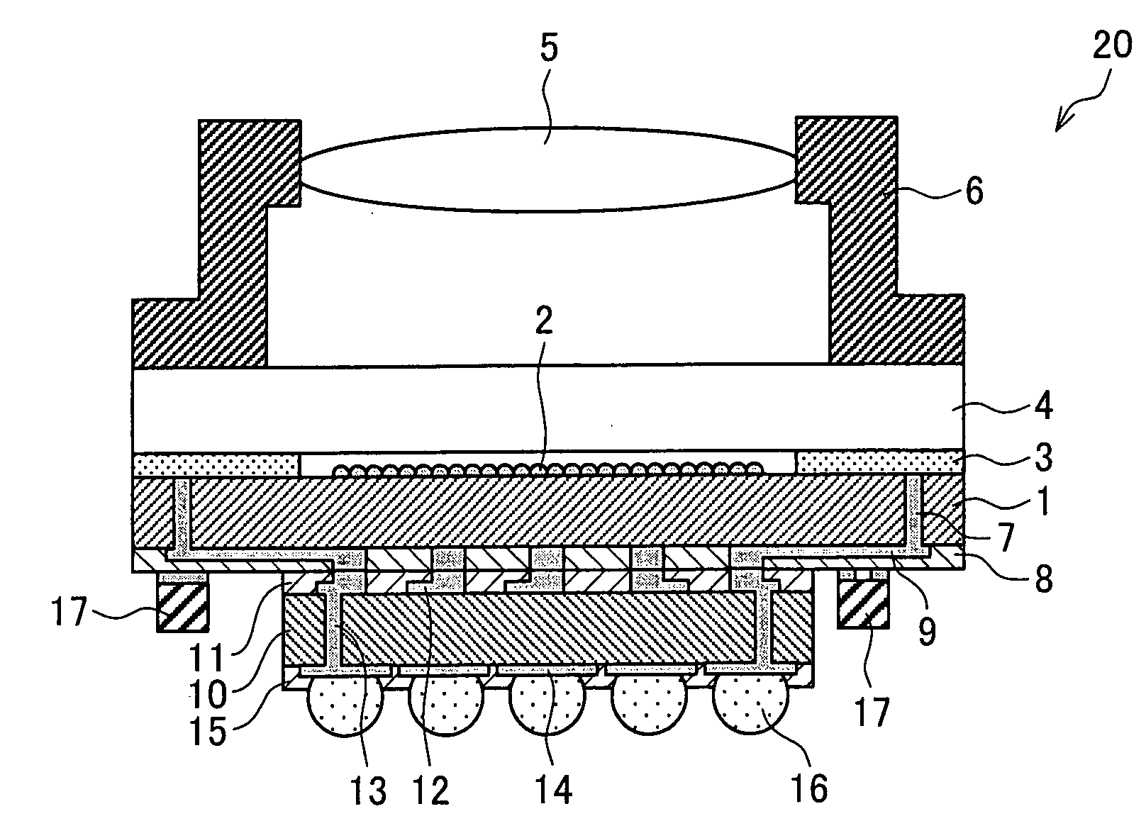
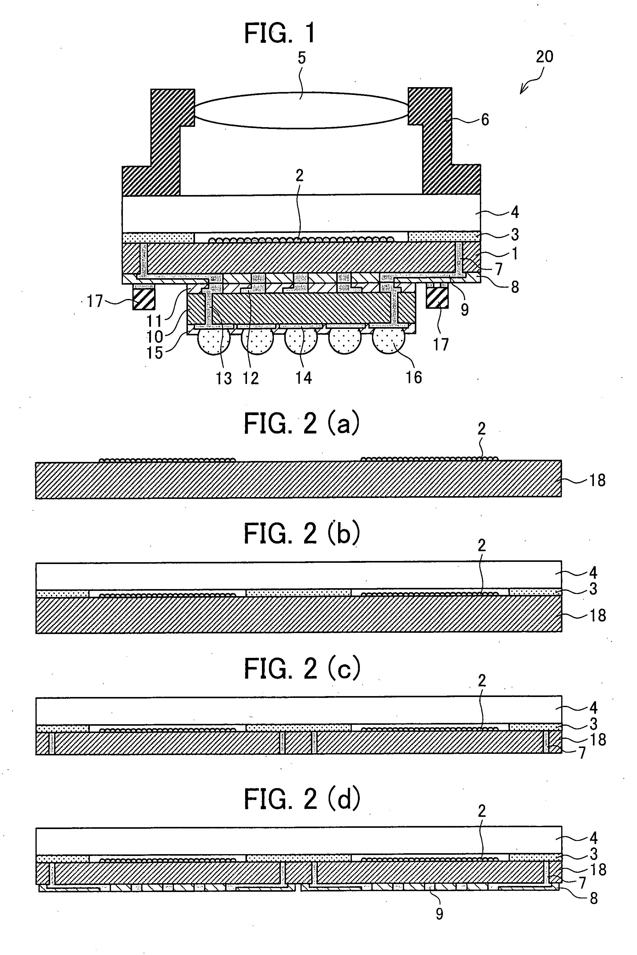
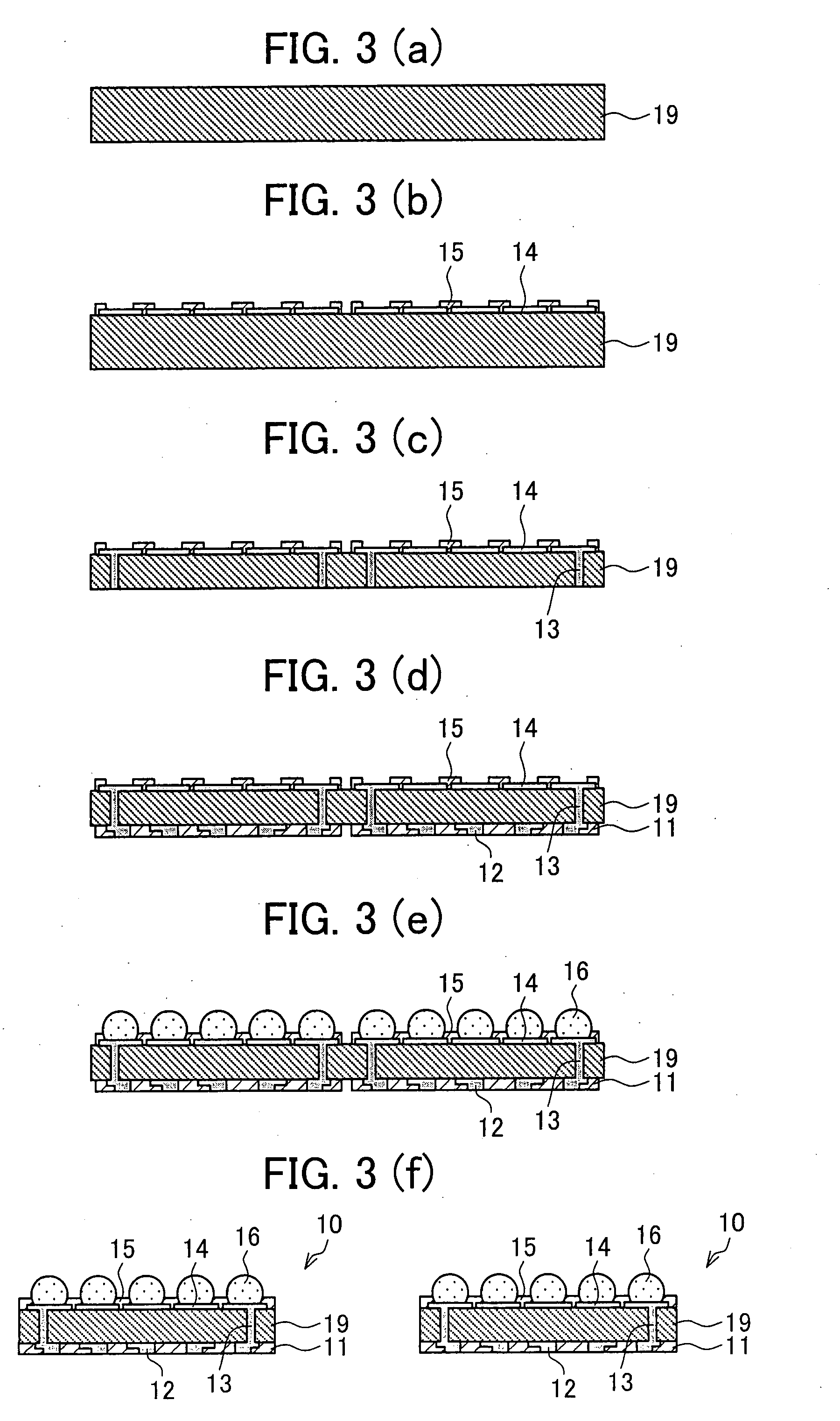
[0042]FIG. 1 is a sectional view showing a structure of a module 20 for an optical apparatus, in accordance with the present embodiment.

[0043]As shown in FIG. 1, the module 20 of the present embodiment includes a solid-state image sensor 1, an image processing apparatus (DSP) 10, a transparent cover section 4, and an optical-path defining unit 6.

[0044]An effective pixel area 2 where photoelectric conversion is to be performed is formed in a central part of one surface of the solid-state image sensor 1. Hereinafter, the surface of the solid-state image sensor 1, on which surface the effective pixel area 2 is formed, will be referred to as a front surface, and an opposite surface to the front surface will be referred to as a rear surface.

[0045]The solid-state image sensor 1 includes, as electric wirings of the module 20, through electrodes (first through electrode) 7 and rear-surface re...


PUM


Abstract

An electric wiring of a module for an optical apparatus includes: a first through electrode passing through the solid-state image sensor; a first rewiring layer being formed in such a way as to be re-wired to a necessary area in the rear surface of the solid-state image sensor, and being electrically connected to the first through electrode; a second rewiring layer being formed in such a way as to be re-wired to a necessary area in the rear surface of the image processing apparatus, and being electrically connected to the first rewiring layer; a second through electrode passing through the image processing apparatus and being electrically connected to the second rewiring layer; and a third rewiring layer being formed in such a way as to be re-wired to a necessary area in a front surface of the image processing apparatus, and being electrically connected to the second through electrode. The image processing apparatus includes an external connection terminal electrically connected to the third rewiring layer. With the foregoing structure, a small and light module for an optical apparatus and a production method of such module are realized without giving a constraint on the structure of the module.

Description

[0001]This Nonprovisional application claims priority under 35 U.S.C. § 119(a) on Patent Application No. 109147 / 2006 filed in Japan on Apr. 11, 2006, the entire contents of which are hereby incorporated by reference.FIELD OF THE INVENTION[0002]The present invention relates to a module for an optical apparatus, which module includes a solid-state image sensor and an image processing apparatus for processing an electric signal supplied from the solid-state image sensor. The present invention also relates to a method of producing the module.BACKGROUND OF THE INVENTION[0003]In recent years, modules for optical apparatuses that are to be installed in optical apparatuses, such as digital cameras and mobile phones with camera functions, have been developed (for example, Japanese Unexamined Patent Publication No. 2002-182270 (publication date: Jun. 26, 2002)).[0004]The following explains, as an exemplary conventional module for an optical apparatus, which module includes a solid-state image...

Claims


Application Information

Patent Timeline
IPC IPC(8): H01L31/0232H01L31/18G02B7/02G03B17/02H04N5/225H04N5/335
CPCH01L27/14618H01L27/14625H01L2924/07811H04N5/2257H04N5/2253H01L2924/3025H01L2924/01079H01L2924/01078H01L27/14685H01L2224/48227H01L2224/48465H01L2924/01029H01L2924/00H04N23/54H04N23/57G02B7/02H01L27/14636
Inventor ONO, ATSUSHI
Owner SHARP KK
Why Eureka
Try Eureka