Method for digitizing an analog quantity, digitizing device implementing said method, and electromagnetic radiation detector integrating such a device

a technology of digital quantity and digitizing device, which is applied in the field of electronic radiation detectors, can solve the problems of limiting the performance of analog-to-digital converter, increasing the sensitiveness of external disturbances, and each of the conversion devices may be sensitive to the generated electrical disturbance, so as to improve the performance of methods and devices, reduce the number of electronic components, reduce the size of the electronic components, and reduce the effect of power consumption

Active Publication Date: 2008-07-24
ULIS SAS
View PDF19 Cites 14 Cited by
  • Summary
  • Abstract
  • Description
  • Claims
  • Application Information

AI Technical Summary

Benefits of technology

[0063]The present invention therefore relates to a method and a device for converting analog quantities to digital signals, which serve to substantially improve the performance of the methods and devices of the prior art. The present invention is aimed in particular to increase the accuracy of the conversion while decreasing the number of electronic components, their power consumption, their size, and the production cost of an analog-to-digital converter, compared with the converters of the prior art.
[0074]Thus, the digitization of the analog quantity to be integrated is broken down into two integration phases (two slopes), for the most significant bits and the least significant bits respectively, thereby serving to digitize the analog quantity rapidly, while using a single comparator. During the second integration phase, the residue to be integrated is evaluated by ignoring the value of the most significant bits, converted to analog, from the analog quantity to be integrated. Moreover, the analog signal representing the least significant bits is amplified with a gain which serves to increase the accuracy, that is, decrease the maximum error, of the second integration phase.
[0076]Thus, the amplification of the residue of the analog quantity to be integrated therefore serves to decrease the maximum error of the second integration phase, hence to decrease the constraint on the accuracy of this analog-to-digital converter.
[0098]In other words, the analog-to-digital converter of the present invention comprises a single operational integrator amplifier and a single operational comparator amplifier. Furthermore, it comprises an analog-to-digital reverse feedback circuit serving to isolate, in the integrated analog quantity, the residual most significant bits, to convert said value to an analog quantity, to subtract it from the initial analog signal, and then to amplify said weak signal in order to increase the accuracy and repeatability of the digitization.
[0100]According to a practical embodiment of the invention, the storage means may comprise a locking circuit memory, better known in the technical field considered as a “latch”, connected to the output of the binary counter. Such a memory has the advantage of occupying a small area.

Problems solved by technology

Furthermore, when use is made of a plurality of high resolution conversion devices on the same circuit, each of the conversion devices may be sensitive to the electrical disturbances generated by the neighboring conversion devices.
In fact, the higher the resolution of a converter, the smaller the voltage difference corresponding to two successive digital values, and in consequence, the more sensitive it is to external disturbances.
However, such a conversion method has drawbacks that are liable to limit the performance of such an analog-to-digital converter.
In fact, on the one hand, there is a technological limit to the maximum clock frequency, and on the other, it is well known that the power consumption of the converter increases with this frequency and may thus become excessive for certain applications.
On the contrary, a single slope “voltage-time” conversion method would give a conversion time that is too long for such a resolution.
In fact, the larger the number of electronic components, the higher their total power consumption and the hotter the circuits become.
Furthermore, the size occupied by these electronic components limits the fineness of the repetition step between two adjacent columns of sensors.
Moreover, the manufacturing capacities are commensurately lower, and hence the manufacturing costs are obviously higher with a larger number of electronic components in a converter.
However, the conversion methods and devices operating the two integration slopes are currently faced with several difficulties which limit their digitization performance.
Firstly, since each column of the matrix detector has its own conversion device, the size thereof limits the reduction of the repetition step, hence the 25 miniaturization of the detector.
In fact, the voltage offset between the thresholds of these two comparators is very low, so that it is difficult to generate reference voltages Vref1 and Vref2 with sufficient accuracy to digitize the least significant bits.
Another difficulty arises from the fact that the comparator 223 designed to digitize the least significant bits operates over a restricted voltage range, making it very sensitive to noise and to electrical disturbances occurring in the circuit, particularly during the switching of the switches 232 and 233.
In particular, in the case of the conversion at the end of each column, a problem of pairing is encountered between transistor power sources when the number of columns is high.
However, these additional electronic components complicate the assembly and above all, increase the area occupied by the conversion device.

Method used


Image

  • Method for digitizing an analog quantity, digitizing device implementing said method, and electromagnetic radiation detector integrating such a device
  • Method for digitizing an analog quantity, digitizing device implementing said method, and electromagnetic radiation detector integrating such a device
  • Method for digitizing an analog quantity, digitizing device implementing said method, and electromagnetic radiation detector integrating such a device

Examples


Embodiment Construction

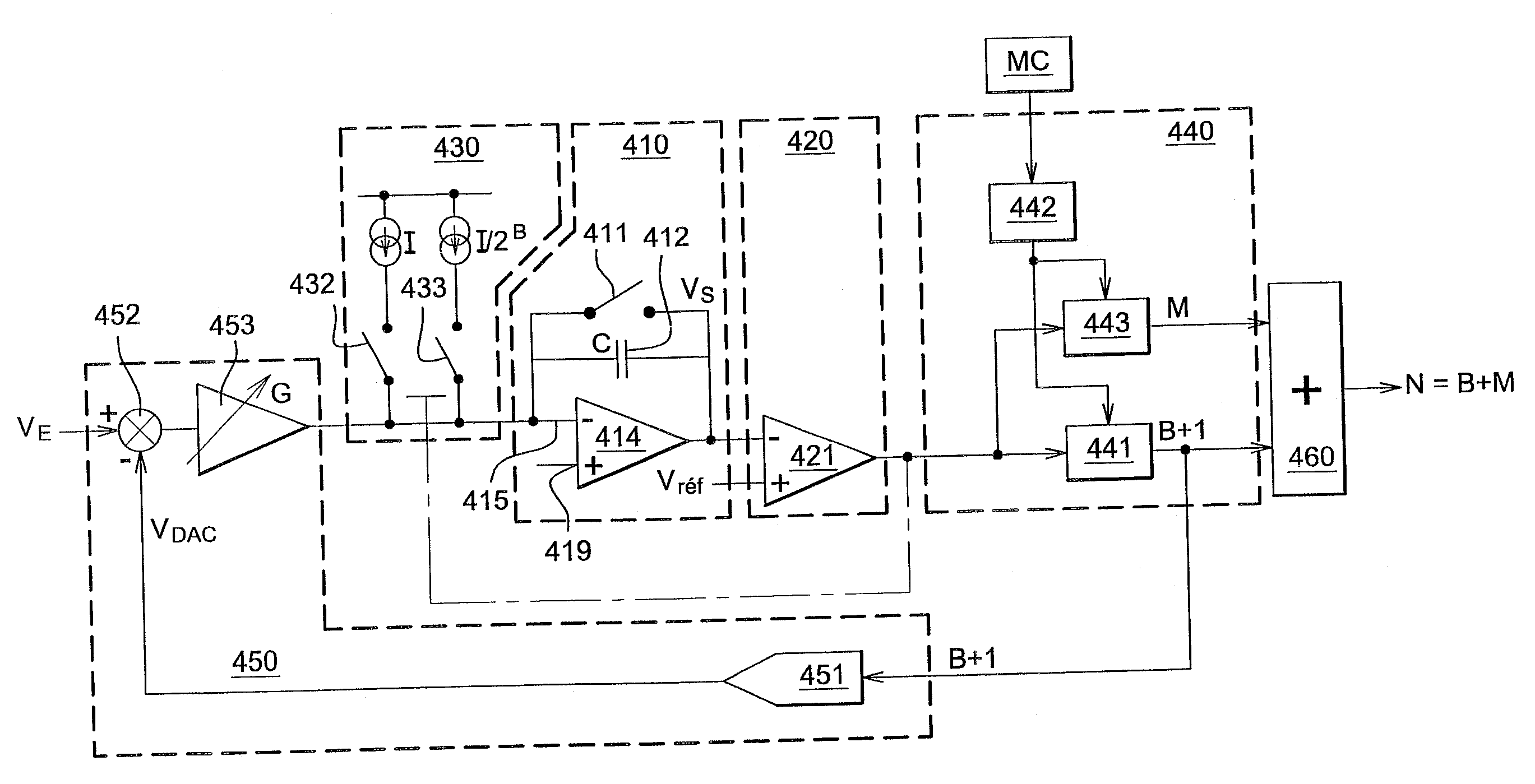
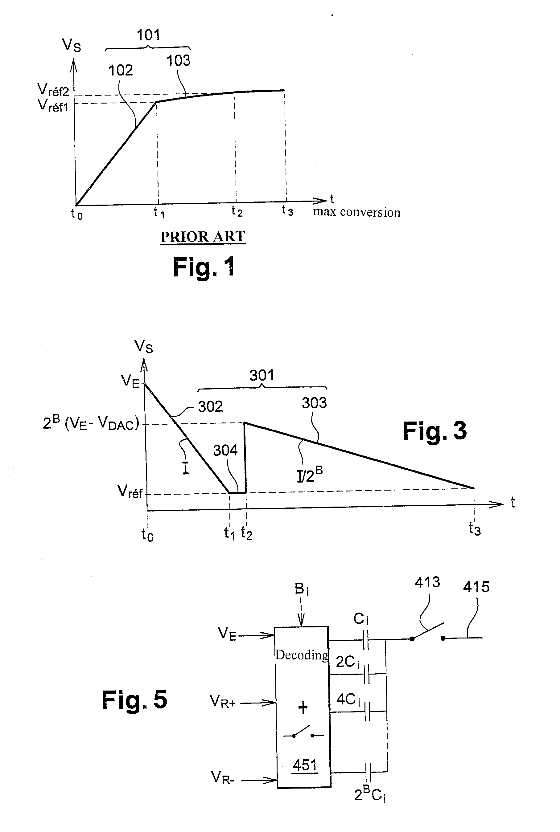
[0113]FIG. 3 shows a timing chart showing the integration of a voltage over time. The x-axis therefore shows the time and the y-axis the voltage. In FIG. 3, the curve 301 thus shows the integration of an input voltage VE, which begins with a first integration phase with a linear ramp 302 and terminates with a second integration phase with a linear ramp 303.

[0114]The integrated analog quantity here is a voltage. This analog quantity could however consist of another electrical quantity representative of the properties displayed by the elementary sensors of the detector during their interaction with the incident radiation. It could accordingly be the quantity of electric charges, for example.

[0115]The times t1 and t2 are separated by a plateau 304 during which the phase called reinitialization is carried out. This reinitialization phase serves to convert the first numerical value representing the most significant bits to an analog signal which is then separated from the analog quantity...


PUM


Abstract

A method of digitizing an analog quantity from an electromagnetic radiation detector including a matrix of juxtaposed elementary sensors, including, for each line or column of the matrix, the steps of: integrating the analog quantity using an integrator stage; converting the integrated analog quantity to a first numerical value via a binary counter and a memory element connected to the output of a comparator stage; converting the first numerical value to an analog signal via an analog-to-digital converter; subtracting the analog signal from the analog quantity to be digitized; amplifying the signal resulting from the subtraction with a gain representing the first numerical value; integrating to produce a second numerical value proportional to the analog signal thereby amplified and forming a second binary number representing the least significant bits; and adding said first and second numerical values to form a number representative of the analog quantity to be integrated.

Description

FIELD OF THE INVENTION[0001]The present invention relates to a method for carrying out the conversion of analog quantities to digital signals, said quantities being in particular produced by an electromagnetic radiation detector. The present invention also relates to a device for carrying out such a conversion.[0002]The present invention therefore relates more generally to the field of electromagnetic radiation detectors, and to the construction and operation of their readout circuit.PRIOR ART[0003]In a manner known per se, electromagnetic radiation detectors are composed of a plurality of juxtaposed elementary sensors in order to form a matrix having a number of lines and columns. The interactions of the incident electromagnetic radiation with these elementary sensors, also called pixels, generate variations of an electrical quantity, corresponding to the energy flux of the incident radiation.[0004]A microbolometric infrared imaging retina is one particular example of such a detect...

Claims


Application Information

Patent Timeline
Patent Type & Authority Applications(United States)
IPC IPC(8): H03M1/12
CPCH03M1/54H03M1/162
Inventor ROBERT, PATRICK
Owner ULIS SAS
Why Eureka
Try Eureka