
Probe for a scanning magnetic force microscope, method for producing the same, and method for forming ferromagnetic alloy film on carbon nanotubes

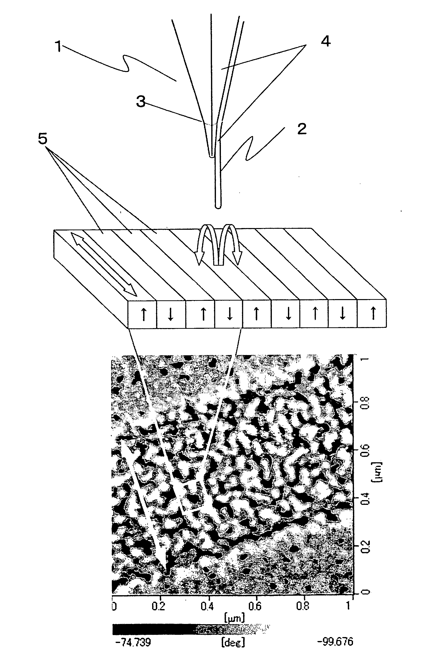
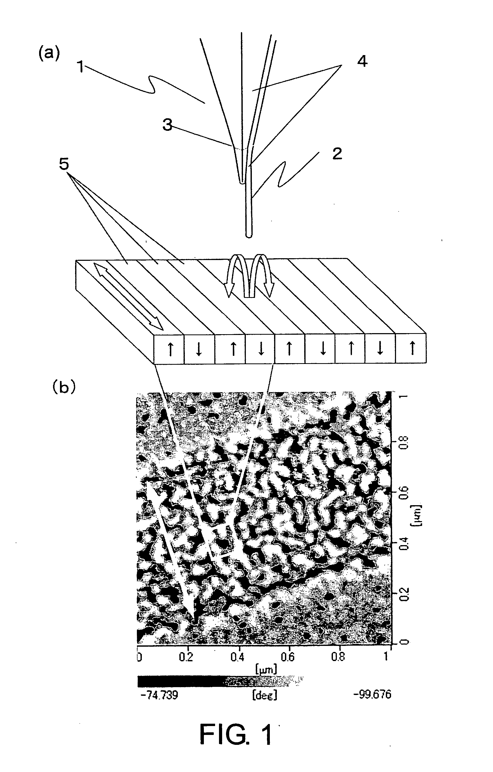
a scanning magnetic force microscope and microscope technology, applied in the direction of material analysis using wave/particle radiation, instruments, nuclear engineering, etc., can solve the problems of insufficient measurement of samples with irregular surfaces, difficult to use carbon nanotubes as scanning magnetic force microscope probes, and conventional probes generally being entirely coated, etc., to improve the directivity of magnetic field, improve the effect of resolution and suppress the leakage of magnetic field

Inactive Publication Date: 2008-07-10
SII NANOTECHNOLOGY INC +1
View PDF8 Cites 2 Cited by
  • Summary
  • Abstract
  • Description
  • Claims
  • Application Information

AI Technical Summary

Benefits of technology

The present invention provides a probe for a scanning magnetic force microscope that uses a carbon nanotube coated with a ferromagnetic alloy film. The coating is stable and does not peel off easily, and the film has a smooth surface to improve resolution. The invention also provides a method for producing the probe with improved magnetic field directivity and resolution. The technical effects of the invention include improved stability, reduced magnetic field leakage, and improved directivity of magnetic field.

Problems solved by technology

However, due to its low rigidity even when attached to a cantilever tip of an AFM, such CNTs have been shown to be inadequate for the measurement of samples with irregular surfaces.
Thus, it has been considered to be difficult to use a carbon nanotube as a probe for the scanning magnetic force microscope.
However, these conventional probes are generally entirely coated.
As a result, they are affected by the information of a wide surface of the sample and, therefore, fail to obtain local information on the probe tip.
Thus, at best, the probe allows for observation of media with highest recording density available at present, and is predicted to be incapable of observing media with much improved recording density.

Method used


Image

  • Probe for a scanning magnetic force microscope, method for producing the same, and method for forming ferromagnetic alloy film on carbon nanotubes
  • Probe for a scanning magnetic force microscope, method for producing the same, and method for forming ferromagnetic alloy film on carbon nanotubes
  • Probe for a scanning magnetic force microscope, method for producing the same, and method for forming ferromagnetic alloy film on carbon nanotubes

Examples


example 1

[0058]A multi-walled carbon nanotube with a diameter of about 10 nm was attached onto a base, and this sample was placed into a sputtering device in which Fe—Co (Fe: 20 at % and Co: 80 at %) sputtering target had been mounted. After Ar gas was introduced at 10 sccm and the gaseous pressure was adjusted to 0.3 Pa, 100 W of radio frequency electric power (RF) was applied to generate plasma. Under this condition (hereinafter referred to as “film formation condition A”), the film-forming treatment was carried out for 4 min and 15 sec.

[0059]The results demonstrated that the Fe—Co ferromagnetic alloy film of the sample had a thickness of 10 nm, as determined from its electron microscopic images. Thus, the mean growth rate of ferromagnetic alloy film was found to be 2.35 nm / min under this condition. The surface roughness of the sample prepared as above was determined at flat portions of the base tip using atomic force microscope. The obtained roughness profile is shown in FIG. 4. The arith...

example 2

[0062]A sample base was prepared through a similar film-forming treatment as described in Example 1, with the exception that the pressure was changed from 0.3 Pa to 1 Pa (hereinafter referred to as “film formation condition B”).

[0063]As a result, the growth rate decreased to 1.48 nm / min, and the surface roughness Ra (L=10 μm) of the formed ferromagnetic film was improved to 0.9996 nm (for comparison, Ra (L=1 μm) was 0.1739 nm). As with the case of Example 1, clear micrographic images could be also obtained for the 1200-kFCI magnetic storage medium.

example 3

[0064]A sample base was prepared through a similar film-forming treatment as described in Example 1, with the exception that the input radio frequency electric power was reduced from 100 W to 50 W (hereinafter referred to as “film formation condition E”).

[0065]As a result, the growth rate decreased to 1.23 nm / min, and the surface roughness Ra (L=10 μm) of the formed ferromagnetic film was improved to 1.046 nm (for comparison, Ra (L=1 μm) was 0.2636 nm). As with the case of Example 1, clear micrographic images could be also obtained for the 1200-kFCI magnetic storage medium.


PUM

PropertyMeasurementUnit
Raaaaaaaaaaa
thicknessaaaaaaaaaa
thicknessaaaaaaaaaa

Abstract

The present invention provides a probe for a scanning magnetic force microscope having a resolution sufficient to allow observation of a magnetic storage medium with 1200 kFCI or higher recording densities, a method for producing the probe, and a method for forming a ferromagnetic alloy film on a carbon nanotube. In the context of the present invention, the probe for a scanning magnetic force microscope comprises a carbon nanotube whose surface is at least in part coated with a ferromagnetic alloy film consisting of any one of a Co—Fe alloy and a Co—Ni alloy, wherein the arithmetic mean roughness (Ra 10 μm) of the surface of the ferromagnetic alloy film is controlled to 1.15 nm or less. A method for producing such probes for a scanning magnetic force microscope and a method for forming such a ferromagnetic alloy film on a carbon nanotube, so as to achieve such mean surface roughness by controlling the growth rate of the ferromagnetic alloy film within the range of 1.0 to 2.5 nm / min, is also disclosed.

Description

FIELD OF THE INVENTION[0001]The present invention relates to a probe for a scanning magnetic force microscope and a method for producing the probe. In particular, it relates to a probe for a high resolution scanning magnetic force microscope to evaluate magnetic storage media on which data has been magnetically recorded at ultra-high density (for example, 1200 kFCI) and a method for producing the probe.[0002]The present invention also relates to a method for forming ferromagnetic alloy film on carbon nanotubes.BACKGROUND OF THE INVENTION[0003]Due to advances in research and development for magnetic storage media represented by recent magnetic hard disks, magnetic storage media with an array of nanomagnets having a thickness of 25 nm or less will soon be available. However, analysis tools for practically evaluating such media are still under investigation. Accordingly, it is currently difficult to achieve thorough evaluation.[0004]Indeed, even in the prior art, while various magnetic...

Claims


Application Information

Patent Timeline
Patent Type & Authority Applications(United States)
IPC IPC(8): B32B9/00C01B31/02G01Q60/54G01Q60/56G01Q70/12
CPCB82Y15/00B82Y30/00B82Y35/00Y10T428/30G01Q70/12Y10S977/842Y10S977/84G01Q60/56
Inventor AKINAGA, HIROYUKISEMBA, YASUYUKIYOKOYAMA, HIROSHIYASUTAKE, MASATOSHIKURAMOCHI, HIROMI
Owner SII NANOTECHNOLOGY INC
Learn More