
Lot traceable printed circuit board

a printed circuit board and traceable technology, applied in the direction of printed circuit aspects, circuit inspection/indentification, instruments, etc., can solve the problems of batch numbers and racks, production lines, batch numbers and almost impossible to trace back flawed pcbs

Active Publication Date: 2008-06-26
NAN YA PRINTED CIRCUIT BOARD CORPORATION
View PDF9 Cites 9 Cited by
  • Summary
  • Abstract
  • Description
  • Claims
  • Application Information

AI Technical Summary

Benefits of technology

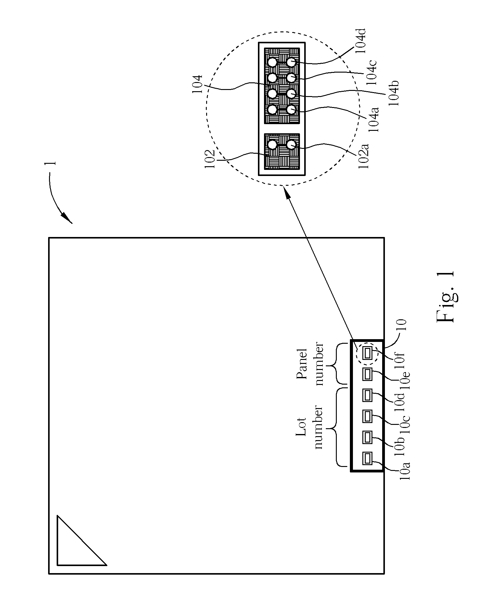
[0009]According to one preferred embodiment of the present invention, the present invention provides a lot traceable PCB which includes a substrate having thereon a patterned circuit layer and a working zone carrying production information related to the PCB per se. The working zone includes a plurality of code boxes, wherein each of the code boxes has a first probe region and second probe region. A single set of resistance test loop is disposed within the first probe region. Four sets of resistance test loops are disposed within the second probe region. A frying probe tester is used to probe the set of resistance test loops respectively for abstracting the production information recorded in the working zone.

Problems solved by technology

However, the current problem is that after the substrate is diced to multiple final PCBs, each final PCB does not possess a corresponding number such as lot number and panel number.
In such a way, it is almost impossible to trace back flawed PCBs regarding the production lines, batch numbers and racks.

Method used


Image

  • Lot traceable printed circuit board
  • Lot traceable printed circuit board
  • Lot traceable printed circuit board

Examples


Embodiment Construction

[0013]FIG. 1 is the top view of the PCB of a preferred embodiment of the present invention. As shown in FIG. 1, PCB 1 may be a final product after dicing and includes patterned circuits (not shown) and a working zone 10 carrying production information such as lot number and panel number. The working zone 10 may be disposed on a periphery region of the printed circuit board 1 or disposed on a region with no patterned circuit layer. In addition, PCB 1 may include an insulation layer such as ABF (Ajinomoto Build-Up) film and a protection layer such as solder-resistant. These are known in the art and will not be described in detail.

[0014]The working zone 10 includes a plurality of code boxes 10a-10f. According to one preferred embodiment of the present invention, the foremost four code boxes, i.e. code boxes 10a-10d, represent lot number and the latter two code boxes, i.e. code boxes 10e-10f, represent panel number. But these illustrations are for example only and not intended to limit ...


PUM


Abstract

A lot traceable printed circuit board (PCB) includes a substrate having thereon a patterned circuit layer and a working zone carrying production information related to the PCB itself. The working zone includes a plurality of code boxes, wherein each of the code boxes has a first probe region and second probe region. A single set of resistance test loop is disposed within the first probe region. Four sets of resistance test loops are disposed within the second probe region. A frying probe tester is used to probe the set of resistance test loops respectively for abstracting the production information recorded in the working zone.

Description

BACKGROUND OF THE INVENTION[0001]1. Field of the Invention[0002]The present invention relates to a printed circuit board. More particularly, the present invention relates to a printed circuit board structure, which facilitates tracing back and identifying the production information of each finished printed circuit board quickly and effectively.[0003]2. Description of the Prior Art[0004]As known by persons of ordinary skill in the art, the manufacturing process of printed circuit boards (PCBs) usually starts with a bulk of substrate as a starting material. First the inner-layer connect is produced to form the necessary layout, which includes pre-treatment, photo-resist application, exposure, development, etching and removal of the photo-resist, then the surface of copper is roughened to increase the adhesion to the insulation resins. Afterwards, they are laminated with plastic sheets. The electric conductivity is accomplished through holes by mechanic or laser means. The inter-substr...

Claims


Application Information

Patent Timeline
Patent Type & Authority Applications(United States)
IPC IPC(8): G06K19/067
CPCH05K1/0266H05K2201/09927H05K2201/09481H05K1/0268
Inventor LO, HSING-LUNLIN, HSIEN-CHIEHCHIANG, KUO-CHUNHO, SHING-FUN
Owner NAN YA PRINTED CIRCUIT BOARD CORPORATION
Learn More