Semiconductor integrated circuit

a technology of integrated circuits and semiconductors, applied in the field of semiconductor integrated circuits, can solve the problems of increasing the development time of the design, the inability to change or add functions, and the inability to execute many commands at the same time, so as to achieve the effect of reducing size, low cost and high performan

Inactive Publication Date: 2008-06-19
RENESAS ELECTRONICS CORP
View PDF5 Cites 13 Cited by
  • Summary
  • Abstract
  • Description
  • Claims
  • Application Information

AI Technical Summary

Benefits of technology

[0004]Because of the wide spread of portable information devices having multimedia processing functions, such as video and sound, and wired and wireless functions, there is a demand to provide such devices reduced in size at low cost by mounting a data processor having high performance, high functionality, and low power consumption. On the other hand, the product value largely depends on quickly meeting various standards established in response to the development of technology. For this reason, it is necessary not only to reduce the product development time but also to extend the product life, by allowing functions to be easily changed or added by software after production.
[0005]Such a data processor may be realized by designing a dedicated logic circuit capable of changing only limited functions prepared in advance like a plurality of operation modes, and mounting a combination of the dedicated logic circuits as a dedicated LSI. Generally, the dedicated LSI could be the best means of realization in terms of achieving high performance and low power consumption. However, the functions may not be changed or added unless the dedicated LSI is redesigned, and the development time for the design may increase.
[0006]Further, the data processor may be realized by mounting a general purpose microprocessor to realize various processings by software including a series of command lines to be executed on the processor. In this case, it is possible to achieve a high functionality, including function change and addition, without changing the hardware of the data processor. However, even in the most-advanced microprocessor, only a few commands can be simultaneously executed. Thus, it is necessary to mount a processor that operates at a very high clock frequency in order to realize processing with high throughput in a data processor based on sequential processing of commands. As a result, the power consumption increases. In addition, a control logic (such as branch prediction) other than the operation is necessary in order to bring out the processing performance of the processor, so that the logic scale of the operation unit itself relatively decreases. As a result, the processing efficiency to the hardware scale may be reduced.
[0009]An object of the present invention is to provide a semiconductor integrated circuit for facilitating the system design.
[0014]According to the present invention, it is possible to provide a semiconductor integrated circuit for facilitating the system design.

Problems solved by technology

However, the functions may not be changed or added unless the dedicated LSI is redesigned, and the development time for the design may increase.
However, even in the most-advanced microprocessor, only a few commands can be simultaneously executed.
As a result, the power consumption increases.
As a result, the processing efficiency to the hardware scale may be reduced.
Thus, although the flexibility is high when a given function is realized in the LSI, the area overhead increases in the application field in which a multi-bit operation such as video and sound processing is mainly performed.

Method used


Image

  • Semiconductor integrated circuit
  • Semiconductor integrated circuit
  • Semiconductor integrated circuit

Examples


Embodiment Construction

1. Typical Embodiment

[0033]First, a typical embodiment of the invention disclosed herein will be summarized. In the summary of the typical embodiment, the reference numerals in the drawings are referred to in parenthesis, which only show the components included the concepts of those designated by the reference numerals.

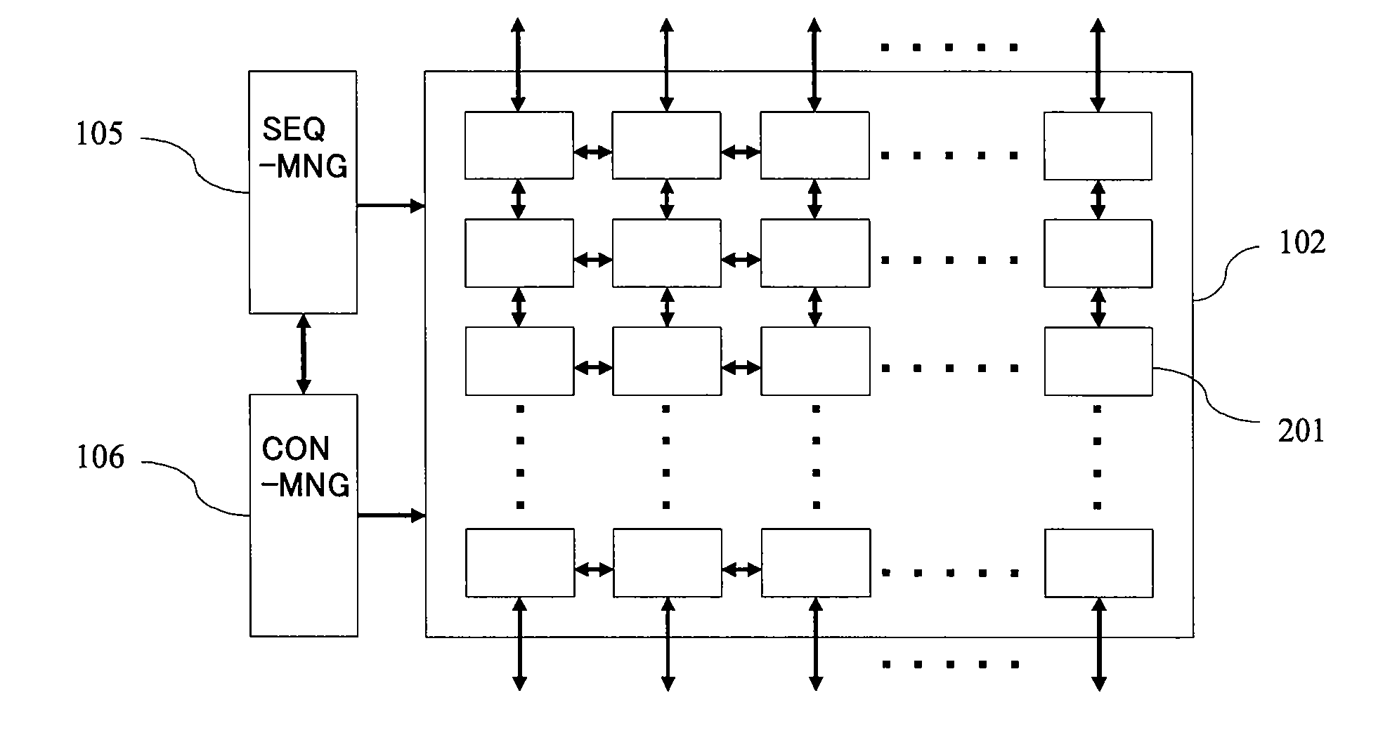
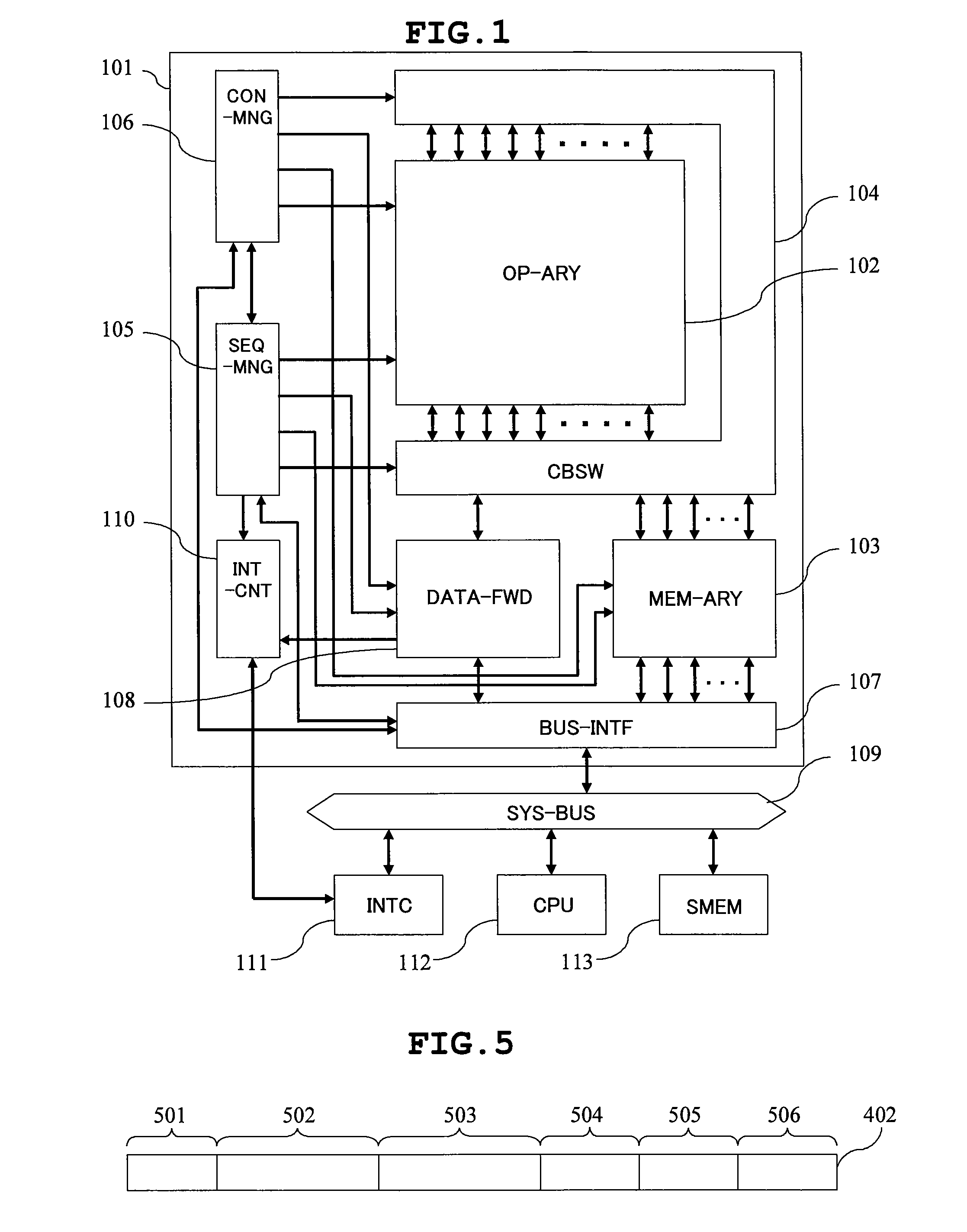
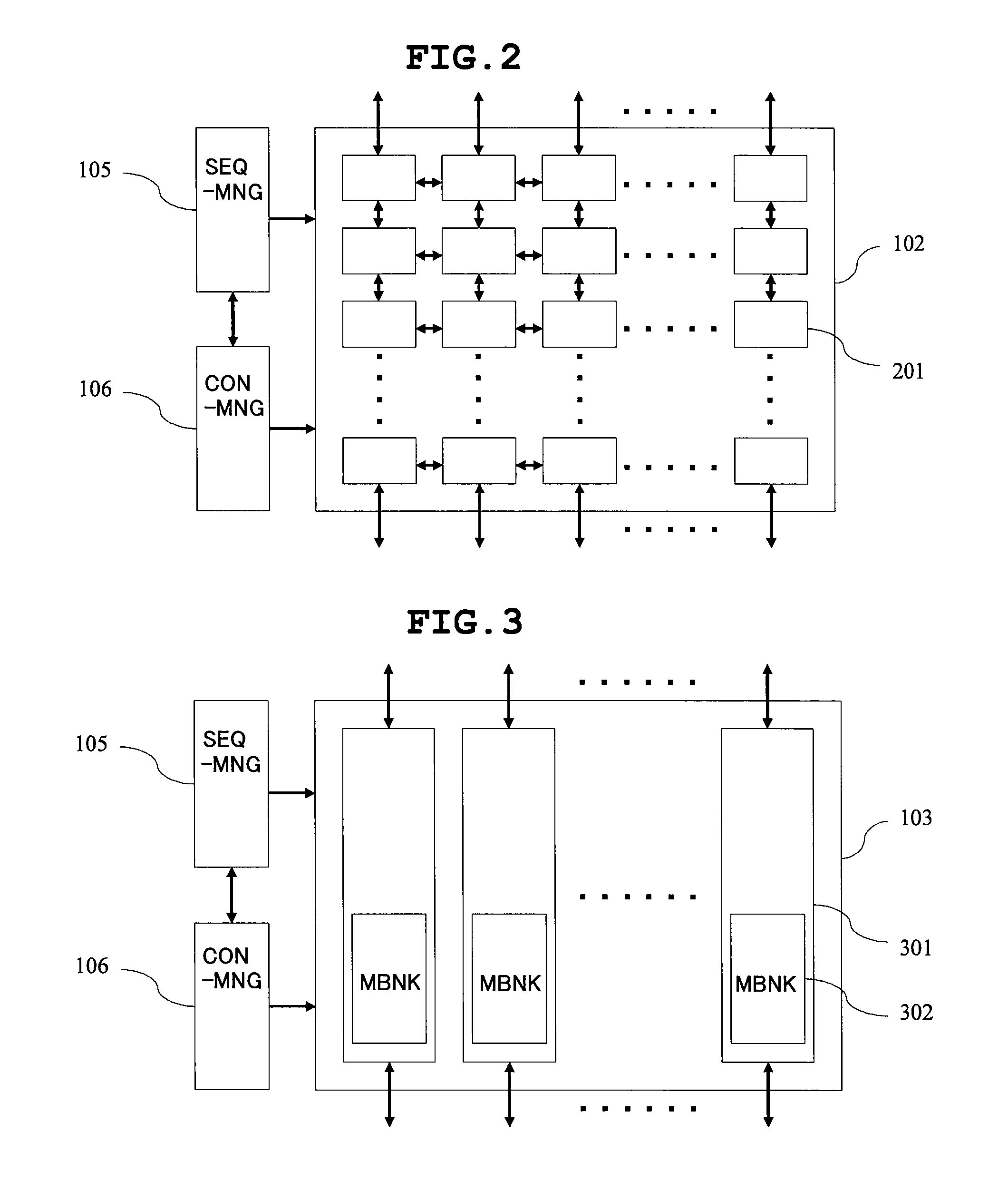
[0034][1] A semiconductor integrated circuit according to the typical embodiment of the present invention, includes an operation unit array (102) formed by arranging a plurality of operation units each capable of performing a predetermined operation; a memory array (103) formed by arranging a plurality of memories each capable of storing data to be operated in the operation unit array; data transfer circuits (108, 701, 1101, 1501) each capable of changing the arrangement of data to be stored in the memory array; and a switch circuit (104) capable of switching data transfer paths between the memory array and the data transfer circuits. The semiconductor integrated circ...


PUM


Abstract

The system design is facilitated by eliminating the increase in data transfer volume of the whole system. In order to facilitate the system design, there are provided an operation unit array, a memory array, a data transfer circuit, and a switch circuit. There are also provided a configuration data management unit for managing the configuration data defining the logical behaviors of the operation unit array, the memory array, the data transfer circuit, and the switch circuit, as well as a state transition management unit capable of controlling the switching of the configuration data. The data transfer circuit includes a control circuit capable of autonomously sorting the data by determining the timing of the data sorting according to the setting included in the configuration data.

Description

CLAIM OF PRIORITY[0001]The present application claims priority from Japanese application JP 2006-337798 field on Dec. 15, 2006, the content of which is hereby incorporated by reference into this application.FIELD OF THE INVENTION[0002]The present invention relates to a semiconductor integrated circuit, and more particularly to a technology which may be effectively applied, for example, to a flexible processor.BACKGROUND OF THE INVENTION[0003]There is known a processor including an operation unit to perform a coarse-grained operation with a width of about 8 to 32 bits as a unit, in which the operation contents and data paths can be changed at high speed to balance the operational performance, circuit utilization ratio, and flexibility at high level. For example, as described in Patent document 1, efficient operation and control can be achieved by independently providing a data path unit for mainly performing operation and a state transition management unit for performing control. The...

Claims


Application Information

Patent Timeline
IPC IPC(8): G06F15/80G06F9/06
CPCG06F15/7867
Inventor KODAMA, TOMOYUKI
Owner RENESAS ELECTRONICS CORP
Why Eureka
Try Eureka