
Method of programming multi-level cells and non-volatile memory device including the same

a multi-level cell and non-volatile memory technology, applied in static storage, digital storage, instruments, etc., can solve the problems of unfavorable multi-level cell programming, unnecessary verification operations with respect to already programmed mlcs, and the configuration of non-volatile memory devices b>50/b> becomes more complicated, so as to prevent unfavorable verification, reduce the integration rate of memory devices, and reduce the total programming time depending on the bits written

Inactive Publication Date: 2008-06-19
SAMSUNG ELECTRONICS CO LTD
View PDF12 Cites 42 Cited by
  • Summary
  • Abstract
  • Description
  • Claims
  • Application Information

AI Technical Summary

Benefits of technology

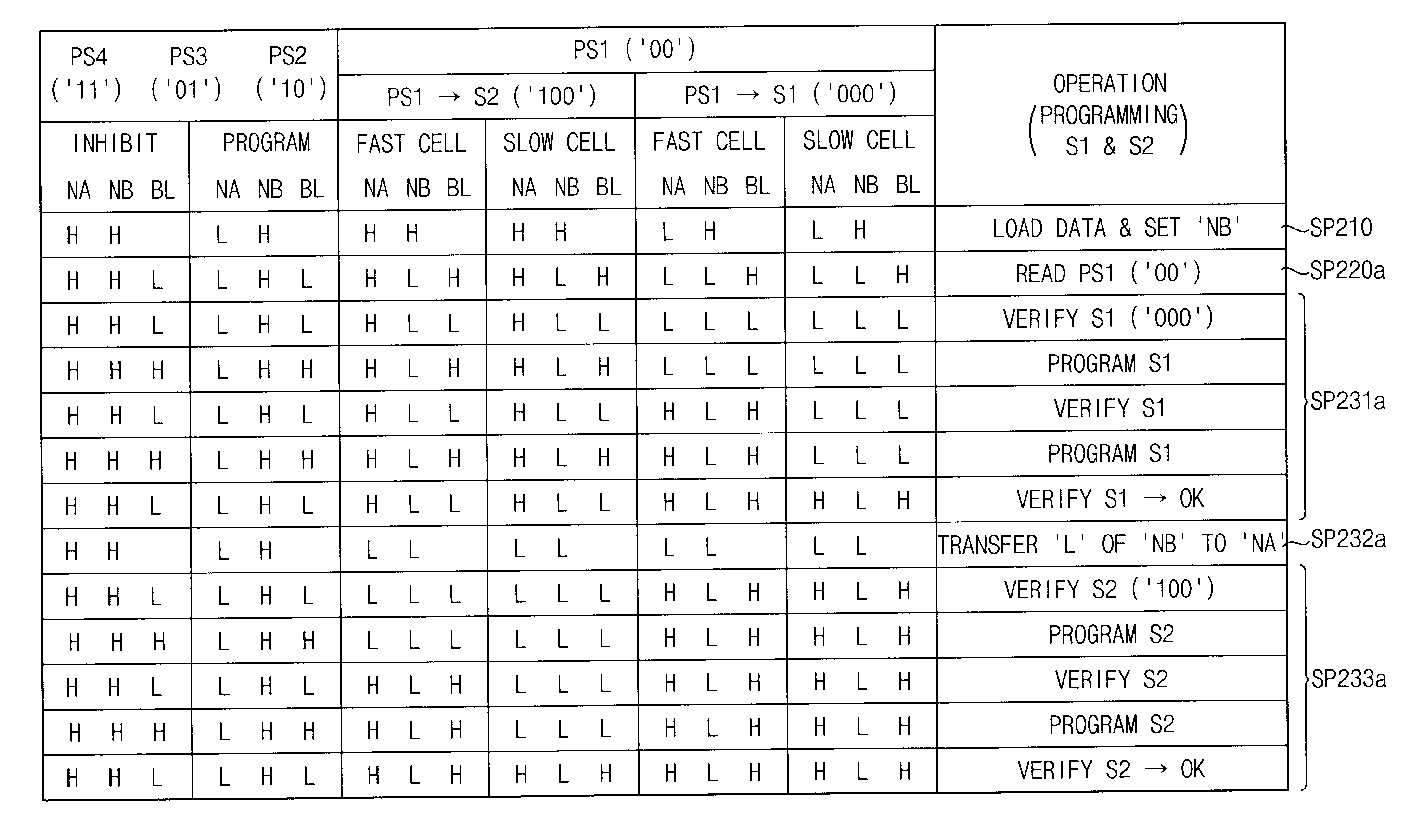
[0059]According to various embodiments, unnecessary verification is prevented since the MLCs are sequentially programmed from the highest threshold voltage to the lowest threshold voltage. Thus, the total programming time depending on bits written in each MLC can be reduced. Also, three or more bits can be written into each MLC using two latches, and thus an integration rate of a memory device can be reduced by implementing a page buffer of a small size.

Problems solved by technology

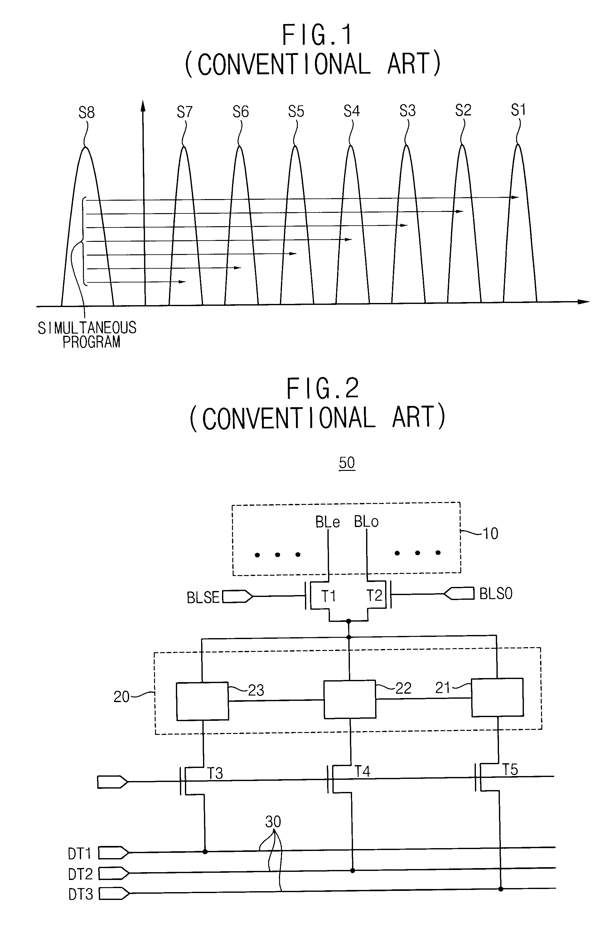
The NAND flash memory device has higher programming and erasing speeds than the NOR flash memory device, but cannot access per byte in a previous state reading operation and programming operation.
Further, configuration of the non-volatile memory device 50 becomes more complicated due to variety of the bitline voltages.
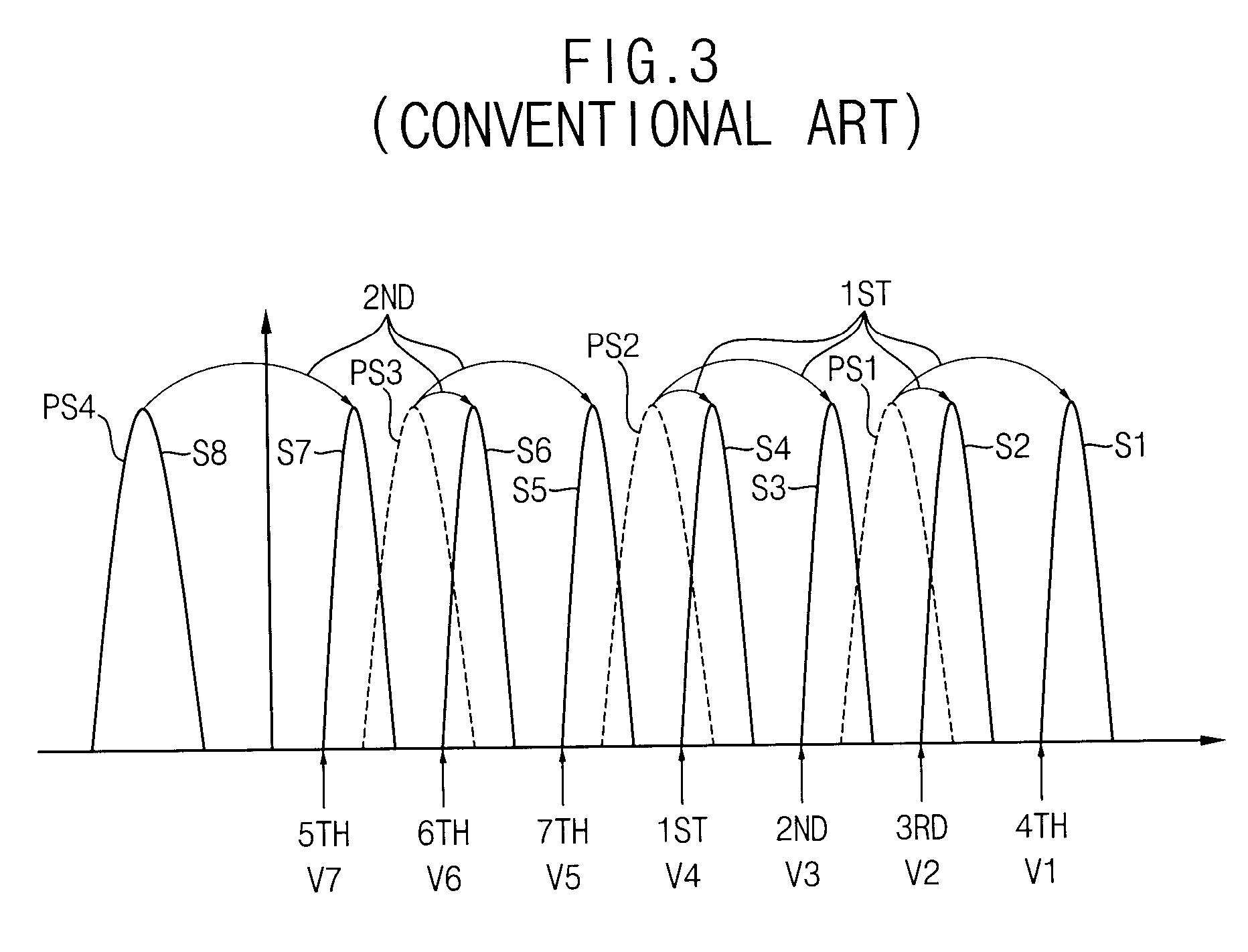
When multiple states are verified after each programming operation, unnecessary verifying operations may occur with respect to already programmed MLCs.
Accordingly, the conventional non-volatile memory devices require complicated configurations.

Method used


Image

  • Method of programming multi-level cells and non-volatile memory device including the same
  • Method of programming multi-level cells and non-volatile memory device including the same
  • Method of programming multi-level cells and non-volatile memory device including the same

Examples


Embodiment Construction

[0079]The present invention will now be described more fully with reference to the accompanying drawings, in which exemplary embodiments of the invention are shown. The invention may, however, be embodied in various different forms, and should not be construed as being limited only to the illustrated embodiments. Rather, these embodiments are provided as examples, to convey the concept of the invention to one skilled in the art. Accordingly, known processes, elements, and techniques are not described with respect to some of the embodiments of the present invention. Throughout the drawings and written description, like reference numerals will be used to refer to like or similar elements.

[0080]It will be understood that, although the terms first, second, etc., may be used to describe various elements, these elements should not be limited by these terms. These terms are used merely to distinguish one element from another. For example, a first element could be termed a second element, a...


PUM


Abstract

A non-volatile memory device has multi-level cells (MLCs), which are programmed such that one page is written in the MLCs having previous states corresponding to at least one previous page. The non-volatile memory device includes a memory cell array, a row selection circuit and a page buffer block. The memory cell array includes the MLCs commonly coupled to a selected word line and respectively coupled to bitlines. The row selection circuit applies sequentially-decreasing read voltages to the selected wordline to read the previous states of the MLCs, and sequentially-decreasing verification voltages to the selected wordline to program states of the MLCs sequentially from a state having a highest threshold voltage to a state having a lowest threshold voltage. The page buffer block loads data corresponding to the one page, and controls a bitline voltage based on each previous state and each bit of the loaded data.

Description

CROSS-REFERENCE TO RELATED APPLICATIONS[0001]A claim of priority is made to Korean Patent Application No. 10-2006-0127578, filed on Dec. 14, 2006, the subject matter of which is hereby incorporated by reference.BACKGROUND OF THE INVENTION[0002]1. Field of the Invention[0003]The present invention relates to programming in a non-volatile memory device, and more particularly to a method of programming multi-level cells, and a non-volatile memory device including the page buffer block.[0004]2. Description of the Related Art[0005]A semiconductor memory device is typically classified into a non-volatile memory device that maintains stored data when power is off, and a volatile memory device that loses stored data when power is off. The non-volatile memory device includes an electrically erasable and programmable read only memory (EEPROM), in which stored data can be electrically erased and new data can be reprogrammed.[0006]Operations of the EEPROM include a program mode for writing data ...

Claims


Application Information

Patent Timeline
IPC IPC(8): G11C16/04
CPCG11C11/5628G11C11/5642G11C2216/14G11C16/3459G11C2211/5621G11C16/0483G11C16/04G11C16/06G11C16/10G11C16/30
Inventor PARK, KI-TAELEE, YEONG-TAEKKIM, KI-NAMKIM, DOO-GON
Owner SAMSUNG ELECTRONICS CO LTD
Learn More