
Multi-bit electro-mechanical memory device and method of manufacturing the same

Inactive Publication Date: 2008-06-19
SAMSUNG ELECTRONICS CO LTD
View PDF20 Cites 38 Cited by
  • Summary
  • Abstract
  • Description
  • Claims
  • Application Information

AI Technical Summary

Benefits of technology

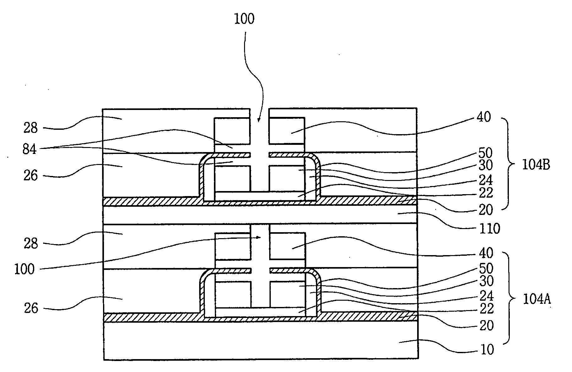
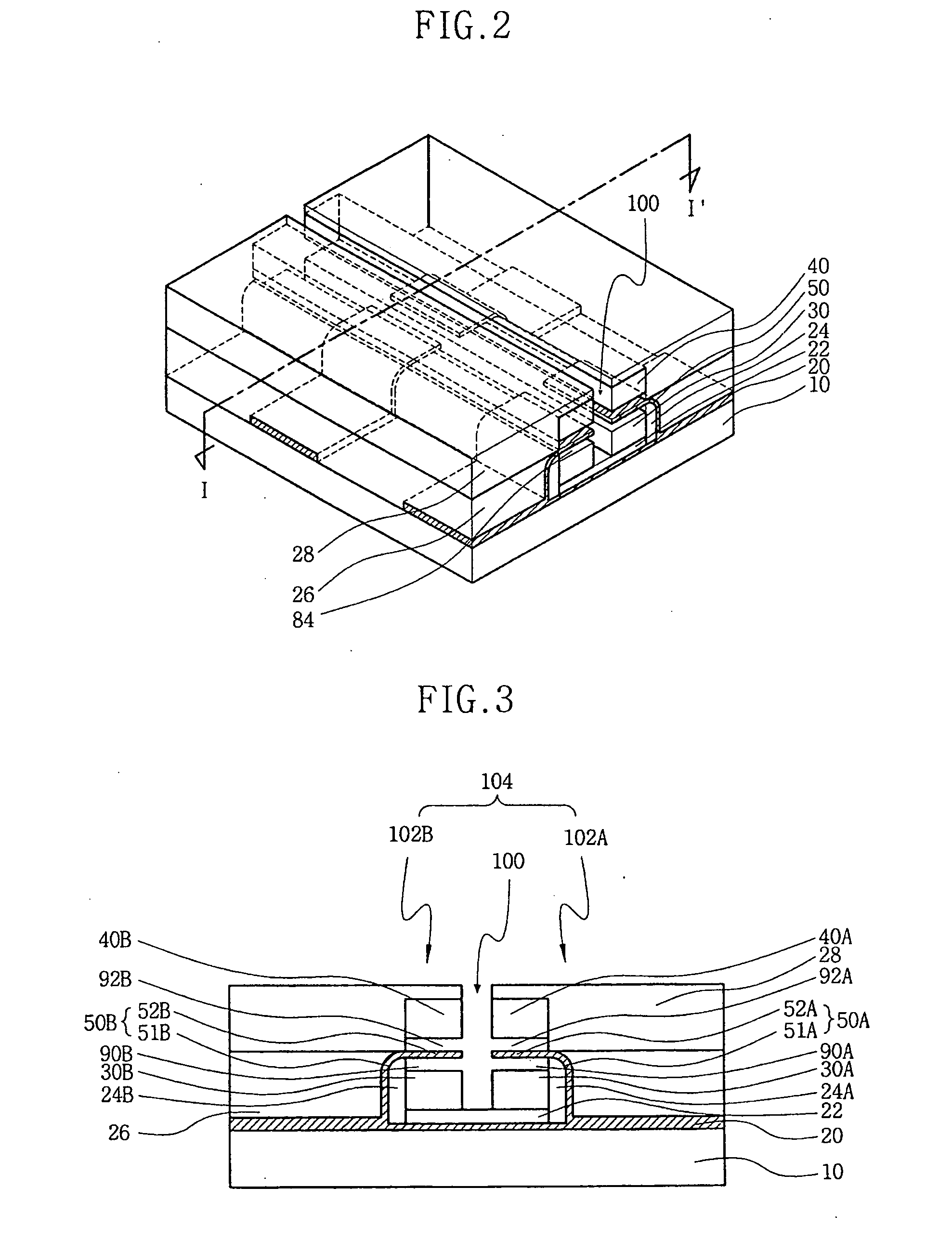
[0016]Embodiments of the present invention provide a multi-bit electro-mechanical memory device, wherein the length of a cantilever electrode is reduced, and a drawing electrode with which the cantilever electrode comes into contact and an FET sensing portion are unified, so that a degree of integration of the device can be enhanced and maximized, and a method of manufacturing the multi-bit electro-mechanical memory device.
[0018]Embodiments of the present invention further provide a multi-bit electro-mechanical memory device, wherein a switching electrode such as a cantilever electrode and a drawing electrode allowing the cantilever electrode to be bent are made of a conductive metallic material with a resistance lower than a poly-silicon material, so that power consumption can be reduced, and a method of manufacturing the multi-bit electro-mechanical memory device.

Problems solved by technology

For this reason, it is difficult to implement a memory device having a nano-graded ultrafine structure.
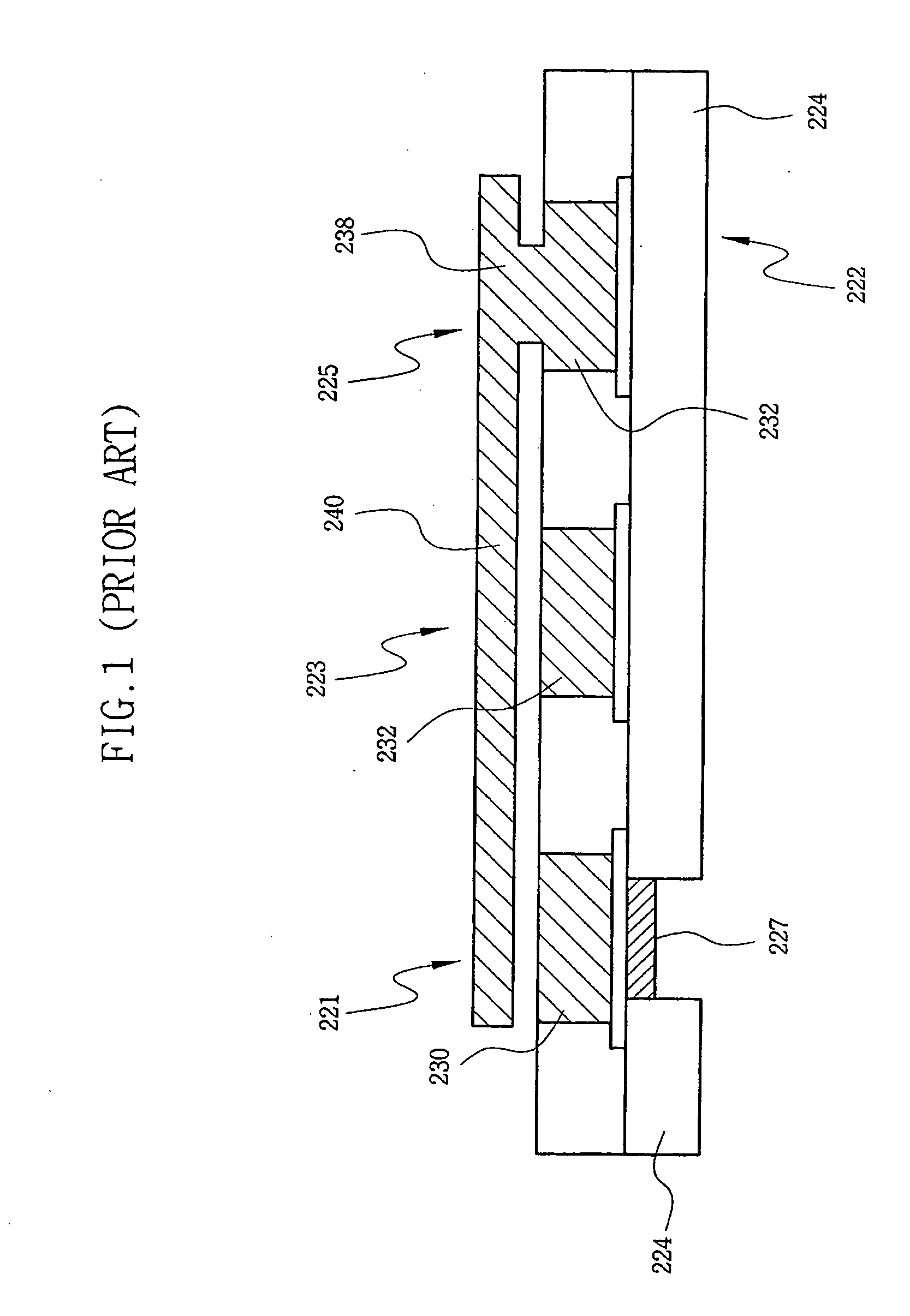
However, the conventional memory device has several disadvantages.
Thus, there is a disadvantage in that a degree of integration of the memory device is lowered.
Thus, it is difficult for multi-bit data to be stored in the conventional memory device.
Thus, power consumption can be undesirably increased.

Method used


Image

  • Multi-bit electro-mechanical memory device and method of manufacturing the same
  • Multi-bit electro-mechanical memory device and method of manufacturing the same
  • Multi-bit electro-mechanical memory device and method of manufacturing the same

Examples


Embodiment Construction

[0045]Hereinafter, aspects of the present invention will be described by explaining illustrative embodiments in accordance therewith, with reference to the attached drawings. While describing these embodiments, detailed descriptions of well-known items, functions, or configurations are typically omitted for conciseness.

[0046]It will be understood that, although the terms first, second, etc. are be used herein to describe various elements, these elements should not be limited by these terms. These terms are used to distinguish one element from another, but not to imply a required sequence of elements. For example, a first element can be termed a second element, and, similarly, a second element can be termed a first element, without departing from the scope of the present invention. As used herein, the term “and / or” includes any and all combinations of one or more of the associated listed items.

[0047]It will be understood that when an element is referred to as being “on” or “connected...


PUM


Abstract

There are provided a multi-bit electromechanical memory device capable of enhancing or maximizing a degree of integration of the memory device and a method of manufacturing the multi-bit electromechanical memory device which includes a substrate, a bit line on the substrate, and extending in a first direction; a word line on the bit line, insulated from the bit line, and extending in a second direction transverse to the first direction, and a cantilever electrode including a shape memory alloy. The cantilever electrode has a first portion electrically connected to the bit line and a second portion extending in the first direction, and spaced apart from the word line by an air gap, wherein the cantilever electrode, in a first state, is in electrical contact with the word line, and, in a second state, is spaced apart from the word line.

Description

CROSS-REFERENCE TO RELATED APPLICATION[0001]This application claims the benefit of Korean Patent Application No. 10-2006-0129884, filed Dec. 19, 2006, the contents of which are hereby incorporated herein by reference in their entirety.BACKGROUND OF THE INVENTION[0002]1. Field of the Invention[0003]The present invention relates to a memory device and a method of manufacturing the same, and more particularly, to a multi-bit electro-mechanical memory device and a method of manufacturing the multi-bit electro-mechanical memory device, in which predetermined data is programmed and read through switching operations of a plurality of cantilever electrodes that are symmetrically formed about a trench.[0004]2. Description of Related Art[0005]In general, memory devices that store information may be classified into volatile memory devices and non-volatile memory devices. Volatile memory devices, which can include dynamic random access memories (DRAMs), static random access memories (SRAMs) or ...

Claims


Application Information

Patent Timeline
IPC IPC(8): G11C11/50H01L21/00
CPCG11C11/56H01L29/788G11C23/00H10B63/80
Inventor LEE, SUNG-YOUNGKIM, DONG-WONKIM, MIN-SANGYUN, EUN-JUNGPARK, DONG-GUN
Owner SAMSUNG ELECTRONICS CO LTD
Learn More