High frequency mos transistor, method of forming the same, and method of manufacturing a semiconductor device including the same
a technology of high-frequency metal oxide semiconductors and transistors, which is applied in the direction of semiconductor devices, electrical equipment, basic electric elements, etc., can solve the problems of affecting the performance of ldmos transistors, fatal signal loss through a channel in real transistors, and breakdown voltages that are generally incompatible with transistor on-resistance, so as to improve transistor electrical characteristics, reduce transistor on-resistance, and reduce the effect of transistor capacitance between the gate structure and drain
- Summary
- Abstract
- Description
- Claims
- Application Information
AI Technical Summary
Benefits of technology
Problems solved by technology
Method used
Image
Examples
embodiment 1
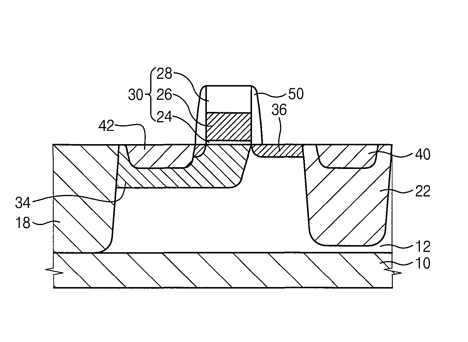
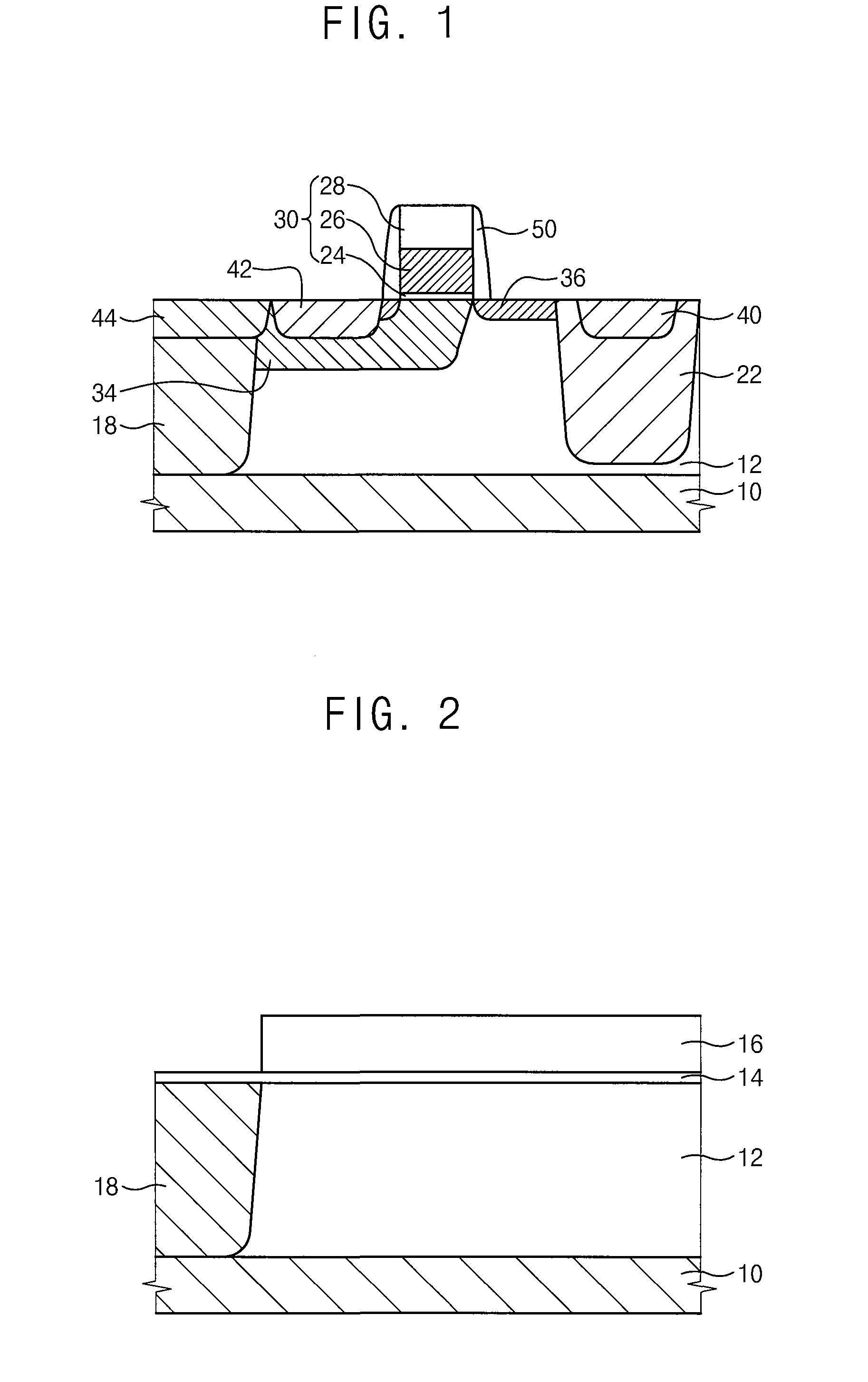
[0043]FIG. 1 is a cross sectional view illustrating a high frequency LDMOS transistor in accordance with a first exemplary embodiment of the present invention.
[0044]Referring to FIG. 1, a semiconductor layer 12 is formed through an epitaxial process on a semiconductor substrate 10 heavily doped with P-type impurities. In the present embodiment, the semiconductor layer 12 on the semiconductor substrate 10 is formed to a thickness in a range from about 1 μm to about 10 μm, and is doped with P-type impurities at a relatively lower concentration than the semiconductor substrate 10.
[0045]A gate structure 30 is formed on the semiconductor layer 12. The gate structure 30 includes a gate insulation pattern 24 having a uniform thickness, a gate electrode pattern 26 and a hard mask pattern 28 that are sequentially stacked on the semiconductor layer 12 in the order named above. A spacer 50 is formed on a side surface of the gate structure 30.
[0046]N-type impurities are implanted at a surface p...
embodiment 2
[0067]FIGS. 7 to 11 are cross sectional views illustrating processing steps for a method of manufacturing a semiconductor device having both a high frequency LDMOS transistor and a CMOS transistor according to a second exemplary embodiment of the present invention.
[0068]Referring to FIG. 7, a semiconductor layer 102 is formed to a thickness of about 1 μm to about 10 μm on a semiconductor substrate 100 heavily doped with P-type impurities through an epitaxial process, and the P-type impurities are implanted through a surface of the semiconductor layer 102 more lightly than the substrate 100 in-situ with the above epitaxial process or in an additional process different from the epitaxial process. In the present embodiment, the semiconductor layer 102 is divided into three distinct regions: an LDMOS region in which the high frequency LDMOS transistor is to be formed, an NMOS region in which an NMOS transistor of a CMOS transistor is formed and a PMOS region in which a PMOS transistor o...
PUM
 Abstract
Description
Claims
Application Information
 - R&D
- Intellectual Property
- Life Sciences
- Materials
- Tech Scout
- Unparalleled Data Quality
- Higher Quality Content
- 60% Fewer Hallucinations
Browse by: Latest US Patents, China's latest patents, Technical Efficacy Thesaurus, Application Domain, Technology Topic, Popular Technical Reports.
© 2025 PatSnap. All rights reserved.Legal|Privacy policy|Modern Slavery Act Transparency Statement|Sitemap|About US| Contact US: help@patsnap.com


