Liquid crystal panel module and liquid crystal display device using the same

a technology of liquid crystal display and panel module, which is applied in non-linear optics, instruments, optics, etc., can solve the problems of troublesome treatment of the many parts in the manufacturing process, connection defects, and difficulties in the separation of the lcd panel and the backlight unit above-mentioned

Active Publication Date: 2008-04-03
BEIHAI HKC OPTOELECTRONICS TECH CO LTD
View PDF11 Cites 29 Cited by
  • Summary
  • Abstract
  • Description
  • Claims
  • Application Information

AI Technical Summary

Benefits of technology

[0033]A first exemplary aspect of the present invention is to provide an LCD panel module in which a printed wiring board can be easily grounded, an LCD device including the LCD panel module.
[0043]Generally, when an LCD panel is transported by itself, strict packing and careful conveyance are needed in order to prevent dust adhesion to the LCD panel and damage thereto. Further at a manufacturing process, the LCD panel and a backlight have to be carefully assembled so as not to adhere to dust and make a scratch. In contrast, in the present invention, at least one of optical sheets and diffusing plates is built in an LCD panel module. As a result, according to the present invention, without using a special protective member, a rear face of the LCD panel can be protected by the optical sheet and the diffusing plate. A configuration for easy grounding of a printed wiring board in the third exemplary feature is almost the same as the second exemplary feature.

Problems solved by technology

Therefore, it is troublesome to treat the many parts in a manufacturing process.
However, the LCD device in which the LCD panel and the backlight unit above-mentioned are separated have some difficulties described below.
(1) a connection defect may occur due to a troublesome grounding work;
(2) damage of an LCD panel and / or a circuit board may occur due to an excessive load in a transportation or an assembling process;
(3) contamination or damage of an LCD panel may occur due to a dust in a transportation or an assembling process.
First, grounding of a printed wiring board is difficult.
When an electromagnetic noise superposes on the printed wiring board, it causes defects such as a malfunction of the LCD device and an abnormal display thereof.
As a result, an assembly process and a maintenance work become troublesome in connecting configuration above-mentioned.
When the work for grounding is carelessly incomplete, an electromagnetic noise cannot be blocked off certainly.
Secondly, the circuit elements such as a driver IC, a flexible substrate and a printed wiring board, and an LCD panel tend to be damaged.
Therefore, since the circuit elements touch other members during transportation, excessive load may be applied on the circuit elements or the members.
During the exchange work, the circuit elements may receive excessive load from handling by an assembly operator and a maintenance engineer and may be damaged.
Thus, the interference (i.e. contact) with other members in the LCD panel during transportation may cause damage, bend or the like in the LCD panel.
In particular, when the size of LCD panel is larger, a weight and the interference thereof increase.
Since transformation and / or distortion tend to occur during transportation of such large LCD panel, the risk of damage such as a warp and a breakage therein may be increased.
When an LCD panel and a backlight unit are assembled in a destination for final assembly, damages may be given to the LCD panel.
Thirdly, an LCD panel may be contaminated by dusts, and an exposed surface thereof may get damaged.
However, even if the LCD panel is manufactured by the clean environment, during transportation for LCD device assembly, assembly of a backlight unit or, lamp exchange work, dusts may adhere on the LCD panel.
In such case, an operator may damage the LCD panel by mistake.

Method used


Image

  • Liquid crystal panel module and liquid crystal display device using the same
  • Liquid crystal panel module and liquid crystal display device using the same
  • Liquid crystal panel module and liquid crystal display device using the same

Examples


first exemplary embodiment

The First Exemplary Embodiment

[0071]A liquid crystal display (LCD) panel module and an LCD device having the LCD panel module according to a first exemplary embodiment of the present invention will be described with reference to FIGS. 1 to 15 herein below.

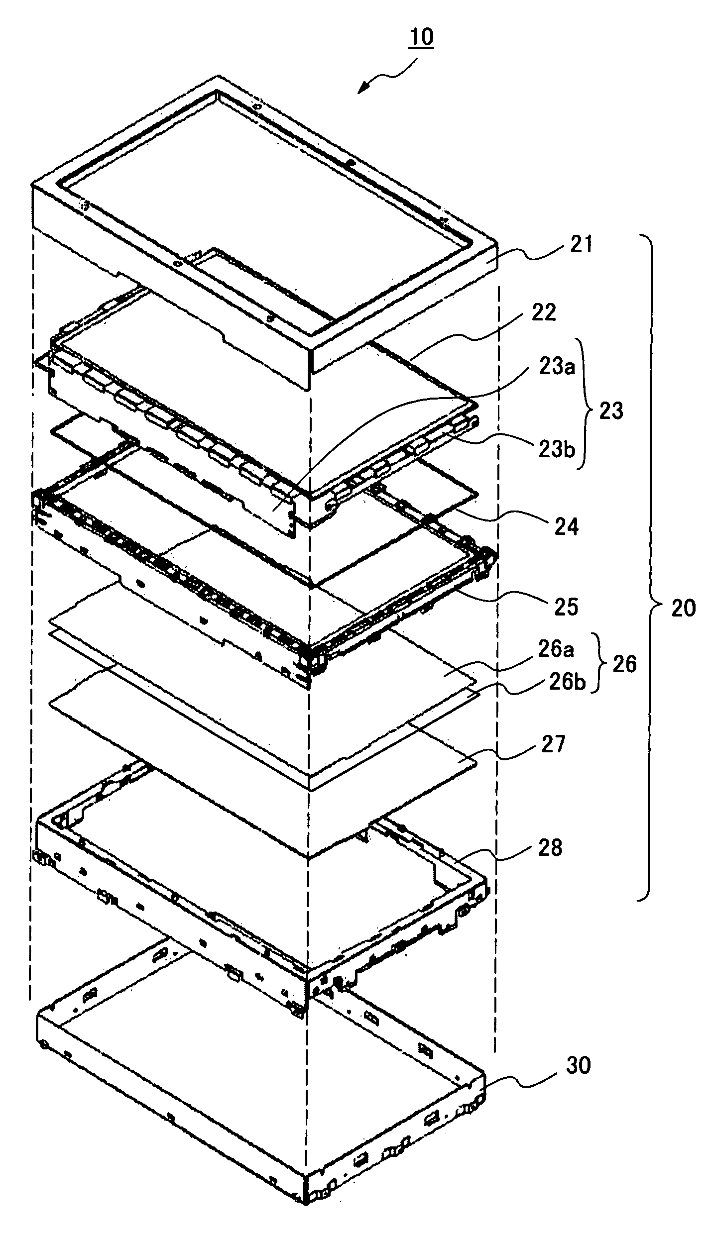
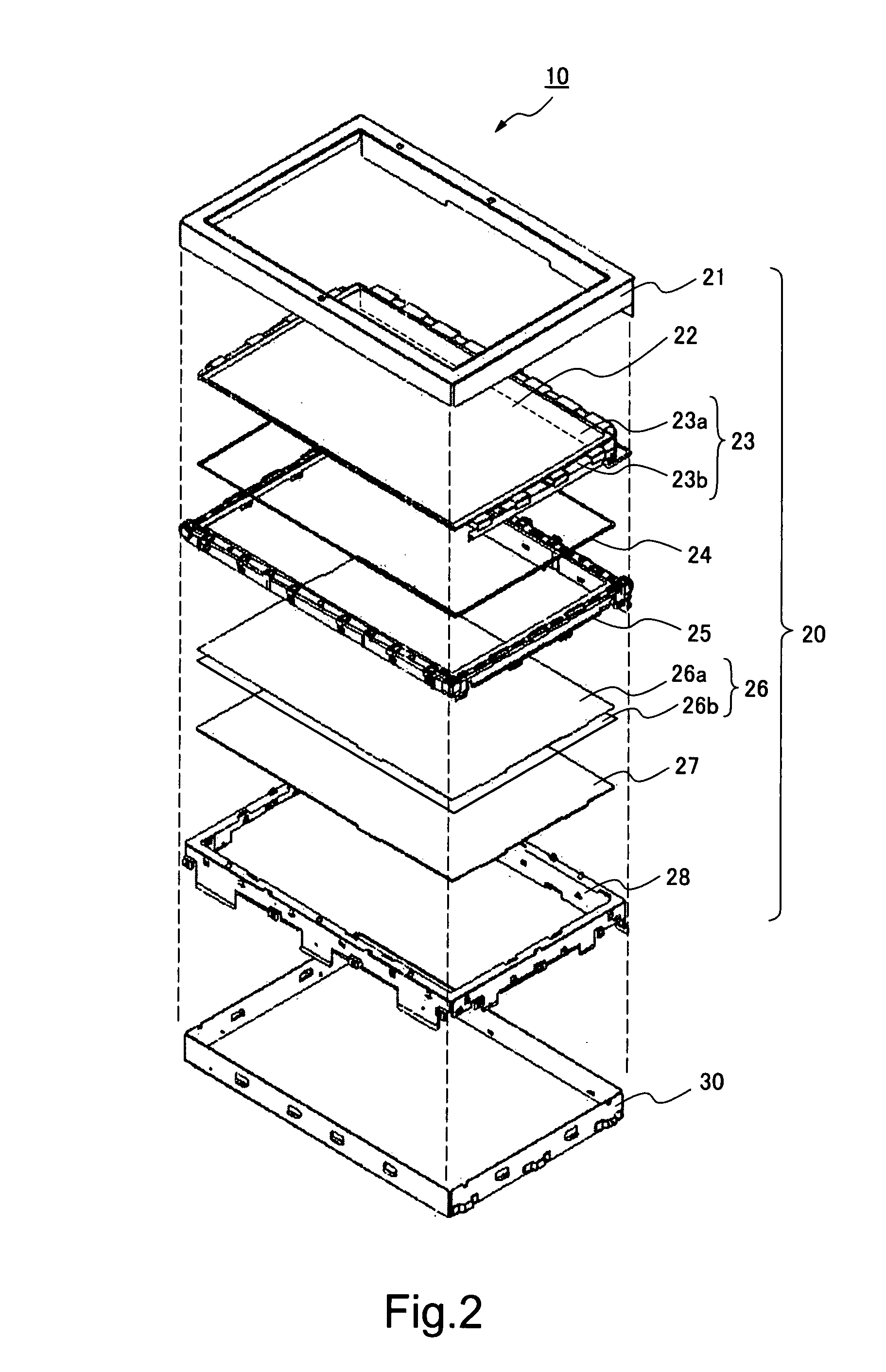
[0072]FIG. 1 is a perspective view showing an appearance of an LCD panel module and a backlight which constitute an LCD device according to a first exemplary embodiment of the present invention.

[0073]As shown in FIG. 1, an LCD device 10 according to the first exemplary embodiment includes an LCD panel module 20 and a backlight 30.

[0074]More specifically, the LCD panel module 20 includes a configuration in which a plurality of members including an LCD panel 22 are integrated into one module. Here, the LCD panel includes members described below:[0075]a first substrate in which a switching element such as a thin film transistor is formed;[0076]a second substrate opposing to the first substrate; and[0077]a liquid crystal (liquid crysta...

second embodiment

The Second Embodiment

[0166]Next, an LCD panel module and an LCD device having the LCD panel module according to a second exemplary embodiment of the present invention will be described with reference to FIG. 16.

[0167]FIG. 16 is a cross sectional view showing an assembling state of an LCD panel module and a backlight according to a second exemplary embodiment of the present invention. In the embodiment, the cross sectional view shows the cross-section approximately taken along X-X line shown in FIG. 1.

[0168]In the first exemplary embodiment mentioned above, in order to protect the LCD panel 22, the optical sheet 26 and the diffusing plate 27 are installed in the LCD panel modules. In the second exemplary embodiment, as shown in FIG. 16, a protective sheet 29, as an example of a protective member, is arranged on a rear side of the LCD panel 22. According to the exemplary embodiment having such structure, contamination and scratch on the LCD panel 22 can be prevented by the protective ...

third embodiment

The Third Embodiment

[0169]Next, an LCD panel module and an LCD device having the LCD panel module according to a third exemplary embodiment of the present invention will be described with reference to FIG. 17 and FIG. 18.

[0170]FIG. 17 is a perspective view showing an appearance of an LCD panel module and a backlight which constitute the LCD device according to the third exemplary embodiment of the present invention. FIG. 18 is a cross sectional view showing an example of a fitting structure of the LCD panel module and the backlight according to the third exemplary embodiment of the present invention, and it shows a cross section taken along Y-Y line shown in FIG. 17.

[0171]In the first exemplary embodiments mentioned above, as shown in FIG. 6, the center chassis 28 of the LCD panel module 20 and the backlight chassis 34 of the backlight 30 are fitted in a normal direction of the display device. However, in the first exemplary embodiment, the printed wiring board 23a is provided in on...


PUM

PropertyMeasurementUnit
electrically conductiveaaaaaaaaaa
electric potentialaaaaaaaaaa
flexibleaaaaaaaaaa

Abstract

Disclosed is a liquid crystal display panel module. The liquid crystal display panel module includes a liquid crystal display panel in which a liquid crystal layer is sandwiched between a pair of substrates facing each other, a printed wiring board which is electrically connected to the liquid crystal display panel, a first frame-shaped chassis which is arranged in front of the liquid crystal display panel, and a second frame-shaped chassis which is electrically conductive and arranged behind of the liquid crystal display panel. In the liquid crystal display panel module, the liquid crystal display panel is held by the first chassis and the second chassis. And, the second chassis and a grounding electrode of the printed wiring board are electrically connected by attaching the printed wiring board to the second chassis.

Description

INCORPORATION BY REFERENCE[0001]This application is based on Japanese Patent Application No. JP 2006-265693 filed on Sep. 28, 2006, and including a specification, claims, drawings and summary. The disclosure of the above Japanese Patent Application is incorporated herein by reference in its entirety.BACKGROUND OF THE INVENTION[0002]1. Field of the Invention[0003]The present invention relates to a liquid crystal display (LCD) panel module which integrates various components such as an LCD panel, and an LCD device including the LCD panel module.[0004]2. Description of the Related Art[0005]An LCD device includes features of a thin shape, a light-weight, and low power consumption. Thus, an LCD device is widely used such as in office automation (OA) equipment, audio video (AV) equipment, portable terminal equipment or the like.[0006]Generally, an LCD device includes a backlight, an optical member, an LCD panel, and a chassis for holding and attaching these members as main components in a...

Claims


Application Information

Patent Timeline
Patent Type & Authority Applications(United States)
IPC IPC(8): G02F1/1333
CPCG02F1/13452
Inventor NISHIMURA, HIDEKI
Owner BEIHAI HKC OPTOELECTRONICS TECH CO LTD
Why Eureka
Try Eureka