Semiconductor device and manufacturing method thereof

a technology of semiconductor devices and manufacturing methods, applied in semiconductor devices, semiconductor/solid-state device details, electrical apparatus, etc., can solve the problems of low degree of freedom for the arrangement of electrodes, restrictions on the miniaturization and high integration of chips, etc., and achieve excellent shielding effects

Inactive Publication Date: 2002-09-12
ACHLYS TECH INC
View PDF0 Cites 2 Cited by
  • Summary
  • Abstract
  • Description
  • Claims
  • Application Information

AI Technical Summary

Benefits of technology

0013] For example, the metal layer may be connected to the grounding potential. This arrangement produces a shielding effect. Further, when this metal layer is utilized as the grounding line, an electrode inside of the element forming area can readily be grounded.
0014] The metal layer may be connected to the power potential. According to this arrangement, the power can readily be fed to an electrode inside of the element forming area. In this case, too, the shielding effect is obtained.
0015] The metal layer may be formed as surrounding the whole periphery of the element forming area. This produces an excellent shielding effect.

Problems solved by technology

This lowers the degree of freedom for the arrangement of the electrodes.
This disadvantageously imposes restrictions on the miniaturization and high integration of chips.

Method used


Image

  • Semiconductor device and manufacturing method thereof
  • Semiconductor device and manufacturing method thereof
  • Semiconductor device and manufacturing method thereof

Examples


Embodiment Construction

[0041] The following description will be made on the assumption that an Si semiconductor is used as the semiconductor type, but it is a matter of course that. a GaAs or Ge semiconductor or other type of semiconductor may also be used.

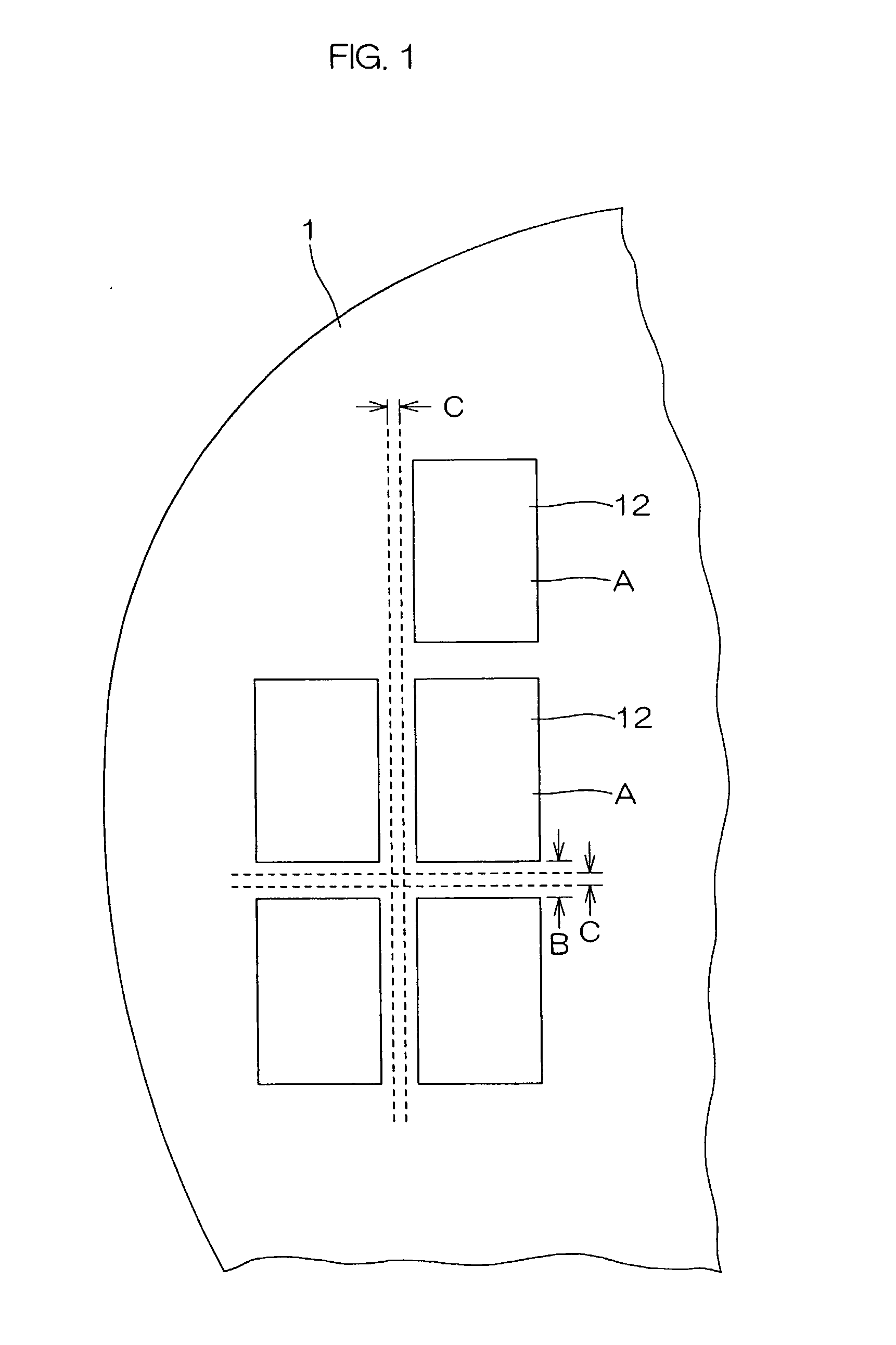
[0042] FIG. 1 is a plan view of an Si semiconductor substrate 1. Arranged on the Si semiconductor substrate 1 are a number of semiconductor elements 12 to be cut into individual chips. Also arranged on the Si semiconductor substrate 1 are a plurality of element forming areas A respectively corresponding to a plurality of semiconductor elements 12. Scribing line areas B serving as allowances to be cut are formed between adjacent element forming areas A. The portions to be actually cut are generally designated by C.

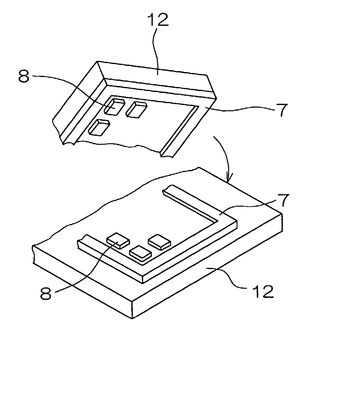
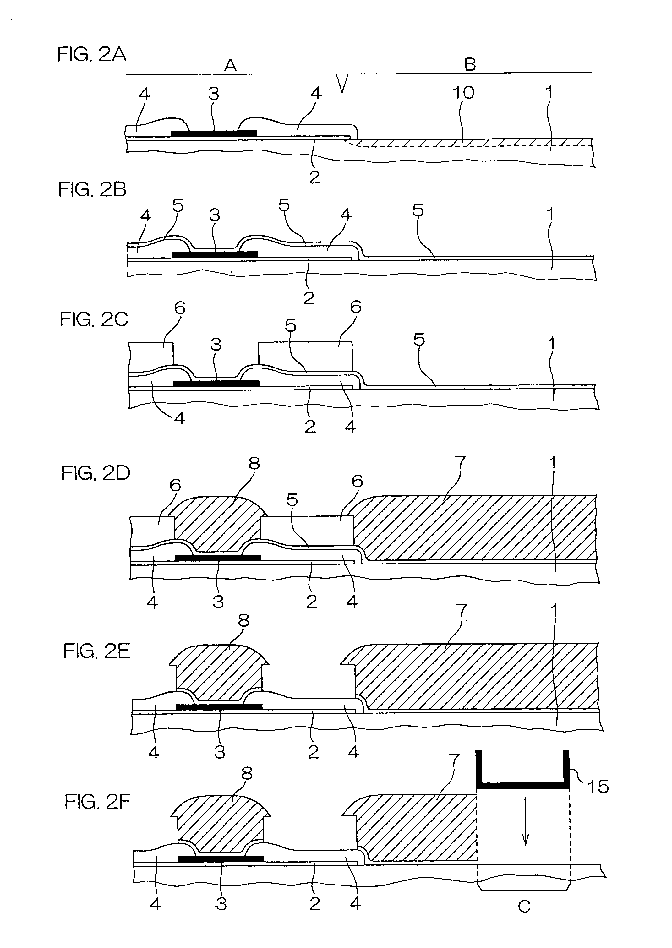
[0043] Each of FIG. 2A to FIG. 2F is a section view of an element forming area A at its peripheral portion for illustrating a bump forming step.

[0044] As shown in FIG. 2A, an Al electrode 3 is formed at a predetermined position of the element f...


PUM


Abstract

A semiconductor device having a metal layer at the peripheral area surrounding an element forming area formed on a semiconductor substrate. This metal layer may be connected to the grounding potential or the power potential. The peripheral area is a scribing line area for example. The metal layer may be formed simultaneously with the formation of a bump within the element forming area.

Description

BACKGROUND OF THE INVENTION[0001] 1. Field of the Invention[0002] The present invention relates to a semiconductor device formed with the use of the peripheral areas (in particular, scribing line areas) of element forming areas, and also to a manufacturing method of such a semiconductor device.[0003] 2. Description of Related Art[0004] When forming semiconductor chips on a wafer, there are formed, around the chips, areas where no elements are formed. These areas serve as allowances to be cut when the chips are cut from the wafer, and are called scribing lines.[0005] Conventionally, such scribing lines are utilized merely as chip cutting allowances.[0006] On the other hand, for disposing bump electrodes or bonding electrodes on a chip, it is required to dispose the electrodes so as to prevent the wirings among the electrodes from getting complicated. This lowers the degree of freedom for the arrangement of the electrodes. This disadvantageously imposes restrictions on the miniaturiza...

Claims


Application Information

Patent Timeline
Patent Type & Authority Applications(United States)
IPC IPC(8): H01L21/301H01L21/60H01L23/485H01L23/50H01L25/065H01L25/07H01L25/18
CPCH01L23/50H01L25/0657H01L2224/1147H01L2224/13099H01L2224/16145H01L2225/06513H01L2225/06551H01L2225/06582H01L2924/01004H01L2924/01013H01L2924/01022H01L2924/01032H01L2924/01046H01L2924/01074H01L2924/01077H01L2924/01078H01L2924/01079H01L2924/01082H01L2924/10329H01L2924/3025H01L2924/01005H01L2924/01006H01L2924/01033H01L2924/01047H01L24/11H01L24/13H01L2224/05022H01L2224/05001H01L2224/05572H01L2924/00014H01L2224/05644H01L2224/05669H01L2224/05099H01L2224/11H01L2224/13H01L2924/00
Inventor HIKITA, JUNICHINAKAGAWA, YOSHIKAZUKUMAMOTO, NOBUHISA
Owner ACHLYS TECH INC
Why Eureka
Try Eureka