
Micro-Fluid Ejection Heads with Multiple Glass Layers

a technology of microfluid ejection and glass layer, which is applied in the direction of printing, inking apparatus, etc., can solve the problems of insufficient use efficiency of circular wafer stock, inability to achieve microfluid ejection heads, and prohibitively expensive cost per chip, etc., and achieve thermal conductivity and smoothness properties suitable

Inactive Publication Date: 2008-04-03
FUNAI ELECTRIC CO LTD
View PDF8 Cites 2 Cited by
  • Summary
  • Abstract
  • Description
  • Claims
  • Application Information

AI Technical Summary

Benefits of technology

[0007]Exemplary embodiments provided in the present disclosure advantageously provide for the manufacture of ceramic substrates having suitable thermal conductivity and smoothness properties to achieve predictable and consistent fluid bubble so as to be suitable for providing micro-fluid ejection heads.
[0008]An advantage of the exemplary heads and methods described herein is that, for example, large array substrates may be fabricated from non-conventional substrate materials including, but not limited to, glass, ceramic, metal, and plastic materials. The term “large array” as used herein means that the substrate is a unitary substrate having a dimension in one direction of greater than about 2.5 centimeters. However, the heads and methods described herein may also be used for conventional size ejection head substrates.

Problems solved by technology

However, the use of silicon substrates has proved unsuitable in achieving micro-fluid ejection heads, such as ink jet heads, having a relatively wide swath from a single piece of silicon.
However, such circular wafer stock is inherently inefficient for use in making large rectangular silicon chips such as chips having a dimension of 2.5 centimeters or greater.
Such a low chip yield per wafer makes the cost per chip prohibitively expensive.
Conventional fabrication processes and wafers have at least some inherent defect density of defects (e.g., impurity concentrations / lattice defects), any of which might cause a device (e.g., a transistor) to fail, thereby effecting the performance and / or usability of the entire head containing that device.
For example, if there are 100 chips on a wafer and 7 such defects, odds are that 6-7 chips will be lost in this fashion, representing a 7% yield loss.
While ceramic materials such as alumina, silicon nitride, and beryllia have adequate thermal conductivity properties, other ceramic and glass materials, such as glass and low temperature co-fired ceramic (LTCC) substrates (which have a significant glass fraction that can be 50% or more) have relatively low thermal conductivities and are unable to effectively dissipate enough heat to prevent overheating of the head, especially if the ejection head is operated at a high frequency.
This inability to effectively dissipate heat can undesirably affect performance of the head.
Another disadvantage of alumina and other ceramic substrates is that it is at best expensive and very technically challenging to achieve the extremely smooth finish which is required for predictable and consistent bubble nucleation.
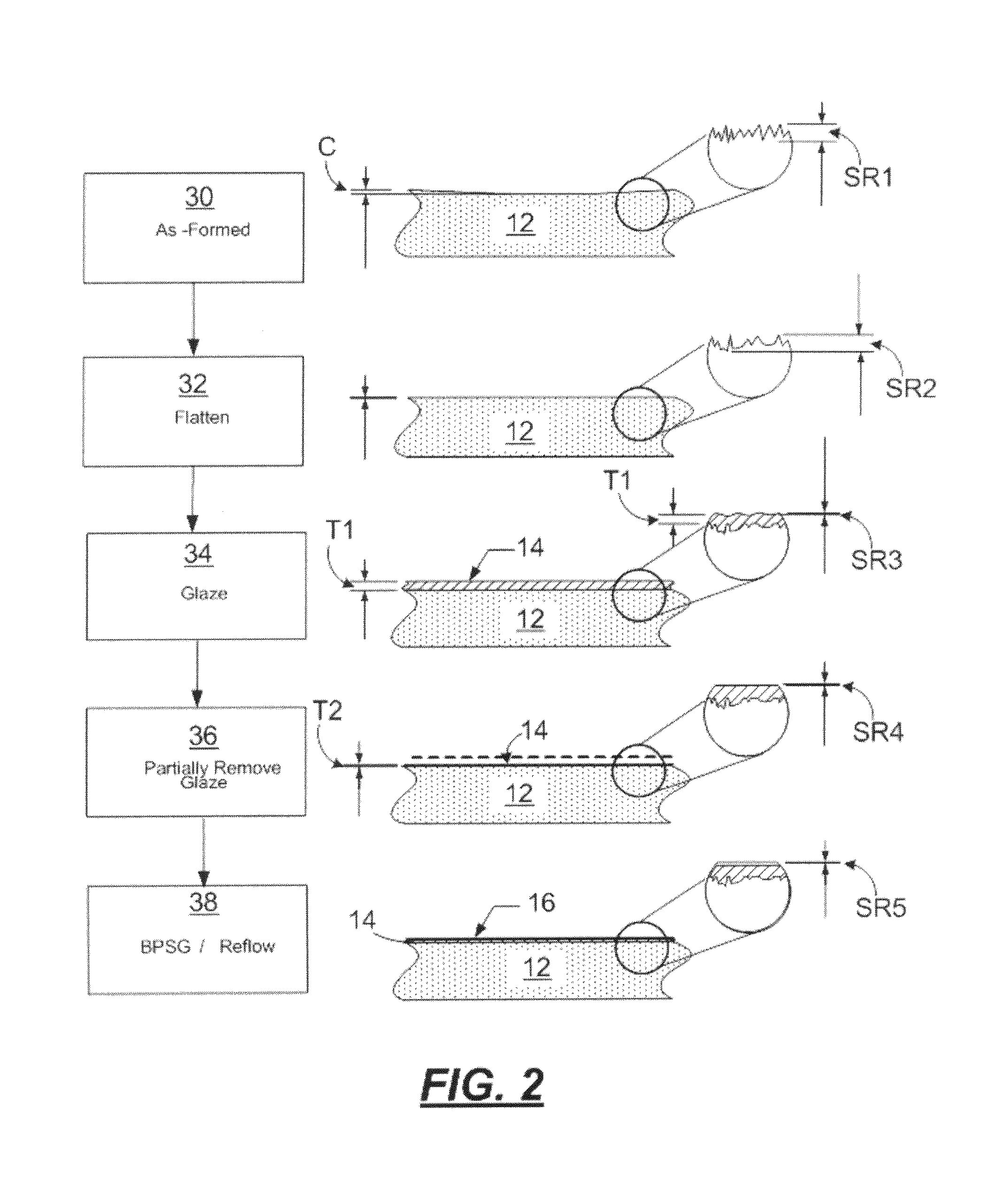
For example, it has been observed that a surface roughness of greater than about 75 Å Ra can contribute to unpredictable and inconsistent bubble nucleation and disadvantageously affect fluid ejection.

Method used


Image

  • Micro-Fluid Ejection Heads with Multiple Glass Layers
  • Micro-Fluid Ejection Heads with Multiple Glass Layers
  • Micro-Fluid Ejection Heads with Multiple Glass Layers

Examples


Embodiment Construction

[0016]As described in more detail below, the exemplary embodiments disclosed herein relate to non-conventional substrates for providing micro-fluid ejection heads. Such non-conventional substrates, unlike conventional silicon substrates, may be provided in large format shapes to provide large arrays of fluid ejection actuators on a single substrate. Such large format shapes are particularly suited to providing page wide printers and other large format fluid ejection devices.

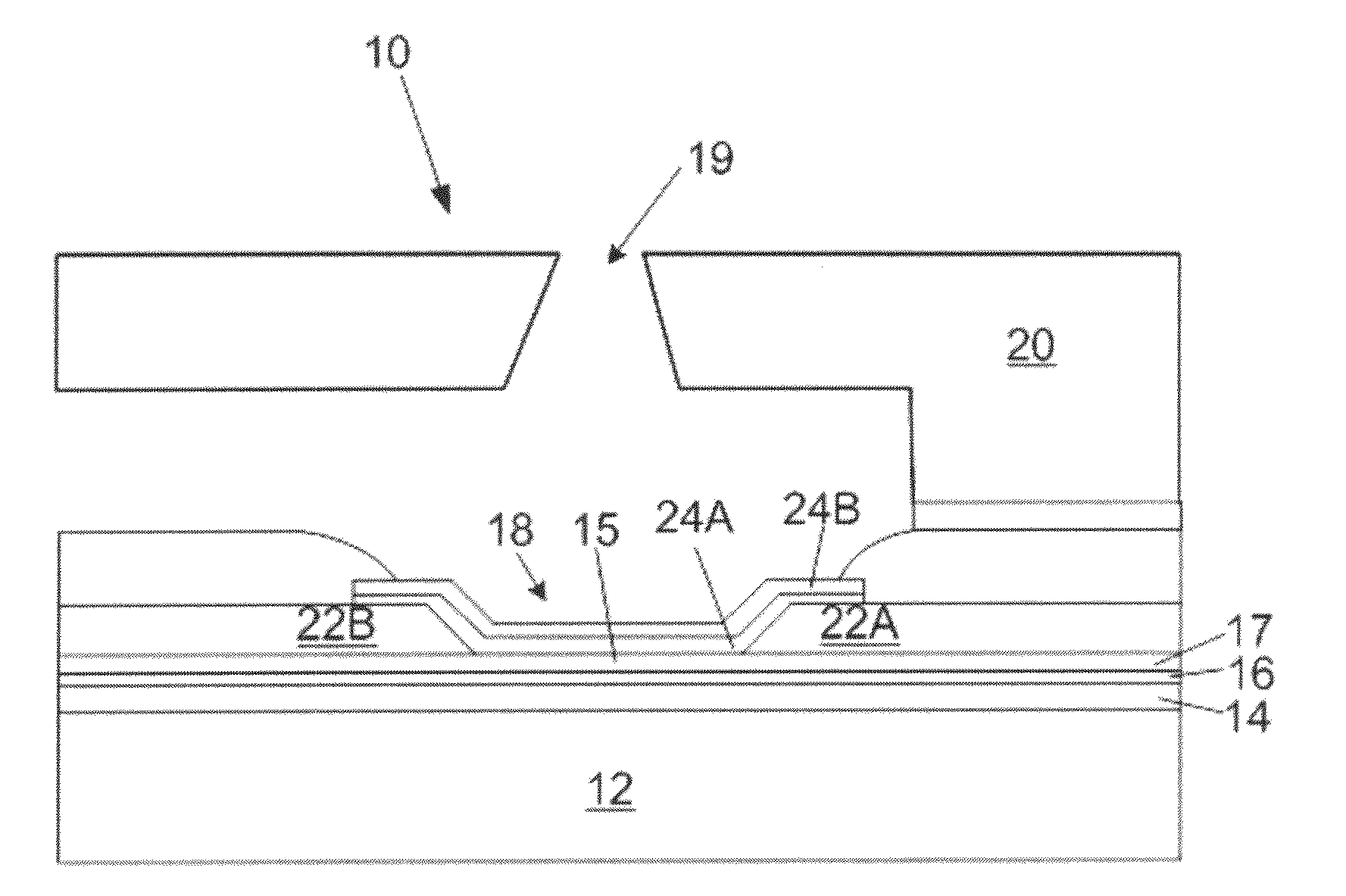
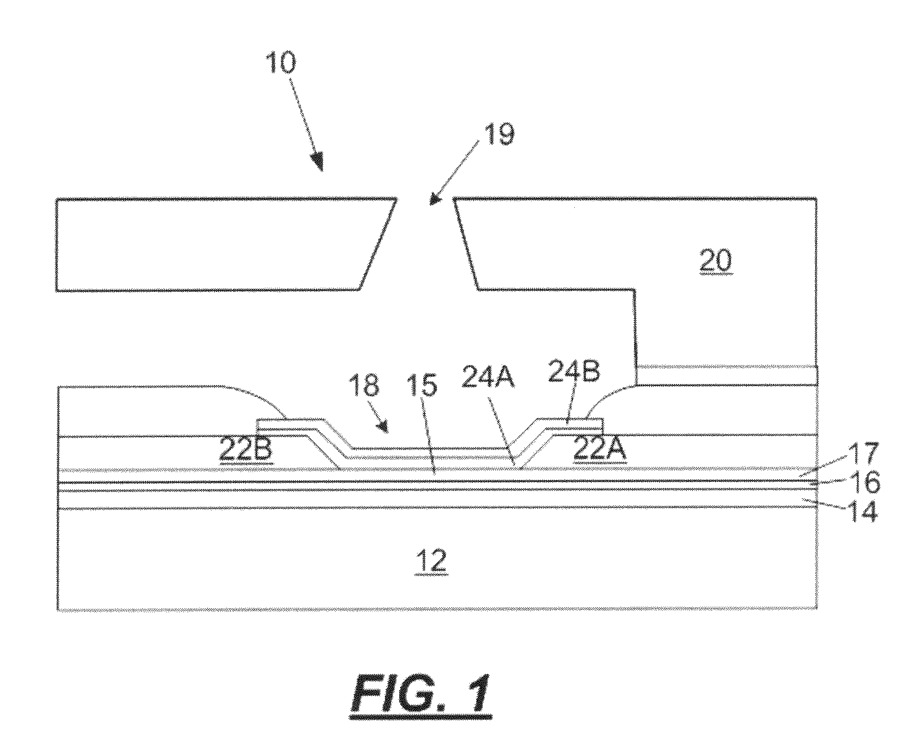
[0017]With reference to FIG. 1, there is shown a plan view of a portion of a micro-fluid ejection head 10, such as an inkjet printhead, having a non-conventional substrate 12 processed to include a first glass layer 14 and a second glass layer 16 according to the disclosure. Such a structure may be used to effectively dissipate heat and provide desirable bubble nucleation characteristics.

[0018]In a manner well known in the art, thermal fluid ejection actuators 15, such as heater resistors are formed from a heater...


PUM

PropertyMeasurementUnit
thicknessaaaaaaaaaa
thicknessaaaaaaaaaa
lengthaaaaaaaaaa

Abstract

Methods for fabricating micro-fluid ejection heads and micro-fluid ejection heads are provided herein, such as those that use non-conventional substrates. One such micro-fluid ejection head includes a substrate having first and second glass layers disposed adjacent to a surface thereof and a plurality of fluid ejection actuators disposed adjacent to the second glass layer. The first glass layer is thicker than the second glass layer and the second glass layer has a surface roughness of no greater than about 75Å Ra.

Description

FIELD OF THE DISCLOSURE[0001]The present disclosure is generally directed toward micro-fluid ejection heads. More particularly, in an exemplary embodiment, the disclosure relates to the manufacture of micro-fluid ejection heads utilizing non-conventional substrates and multiple glass layers.BACKGROUND AND SUMMARY[0002]Multi-layer circuit devices such as micro-fluid ejection heads have a plurality of electrically conductive layers separated by insulating dielectric layers and applied adjacent to a substrate. Thermal energy generators or heating elements, usually resistors, are located on a surface of the substrate to heat and vaporize the fluid to be ejected.[0003]Conventionally, the substrate material has been silicon, and the heads have been fabricated on typically round single crystalline silicon wafers. Silicon has favorable thermal conductivities such that heat is rapidly dissipated from the heater region. Silicon is also capable of accepting (or being polished to) a smooth fini...

Claims


Application Information

Patent Timeline
Patent Type & Authority Applications(United States)
IPC IPC(8): B41J2/06
CPCB41J2/14129B41J2/1603B41J2/1628Y10T29/49083B41J2/1632B41J2202/03B41J2/1631
Inventor CORNELL, ROBERT WILSONDIXON, MICHAEL JOHNDROEGE, CURTIS RAYKLEMO, ELIOSMCKINLEY, BRYAN DALE
Owner FUNAI ELECTRIC CO LTD
Learn More